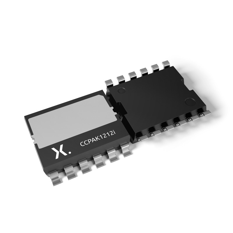
Top-side and bottom-side cooling
For added flexibility in designs and to further improve heat dissipation, CCPAK is available in both top-side cooling and traditional bottom-side cooling package designs.
The first in the portfolio of GaN SMD packages, the CCPAK1212 and CCPAK1212i have a compact footprint of only 12 x 12 mm and a low package height of 2.5 mm.
 |  |
CCPAK GaN FETs videos
Copper-clip SMD CCPAK GaN FET package in half-bridge evaluation board
主要特性和优势
Features and benefits
- Copper-clip
- 3 times lower inductances than industry-standard packages for lower switching losses and EMI
- Higher reliability compared to wire-bond solution
- Thermal performance
- Low Rth(j-mb) typ (<0.5 K/W) for optimal cooling
- 175 °C Tj max
- Manufacturability and robustness
- Flexible leads for temperature cycling reliability
- Flexible gull winged leads for robust board level reliability
- Compatible with SMD soldering and AOI
- Two cooling options
- Bottom-side cooling (CCPAK1212)
- Top-side cooling (CCPAK1212i)
- Plan for Qualifications
- AEC-Q101
- MSL1
- Halogen free
关键应用
Applications
- Automotive EV
- On board charging
- DC-to-DC converters
- Traction inverters
- Industrial
- Telecom and server Titanium grade power supplies
- Industrial vehicle charging
- Solar (PV) inverter
- AC servo drive / Frequency inverters
- Battery storage/UPS inverters
Parametric search
 数据加载中,请稍候...
Products
GaN FETs
| 型号 | 描述 | 状态 | 快速访问 |
|---|---|---|---|
| GAN039-650NBB | 650 V, 33 mOhm Gallium Nitride (GaN) FET in a CCPAK1212 package | Production | |
| GAN039-650NTB | 650 V, 33 mOhm Gallium Nitride (GaN) FET in a CCPAK1212i package | Production |
No Category Data
| 型号 | 描述 | 状态 | 快速访问 |
|---|---|---|---|
| GAN039-650NBB | 650 V, 33 mOhm Gallium Nitride (GaN) FET in a CCPAK1212 package | Production | |
| GAN039-650NTB | 650 V, 33 mOhm Gallium Nitride (GaN) FET in a CCPAK1212i package | Production |
Documentation
| 文件名称 | 标题 | 类型 | 日期 |
|---|---|---|---|
| AN90004.pdf | Probing considerations for fast switching applications | Application note | 2019-11-15 |
| AN90006.pdf | Circuit design and PCB layout recommendations for GaN FET half bridges | Application note | 2019-11-15 |
| RS3138_SOT8005_Combi_2_scr.jpg | CCPAK1212i (SOT8005) package image | Marcom graphics | 2020-05-26 |
| AN90005.pdf | Understanding Power GaN FET data sheet parameters | Application note | 2020-06-08 |
| TN90004.pdf | An insight into Nexperia Power GaN technology – Applications, quality, reliability and scalability | Technical note | 2020-07-21 |
| nexperia_whitepaper_gan_need_for_efficient_conversion.pdf | White paper: Power GaN technology: the need for efficient power conversion | White paper | 2020-07-23 |
| nexperia_whitepaper_gan_need_for_efficient_conversion_CHN.pdf | 白皮书: 功率GaN技术: 高效功率转换的需求 | White paper | 2020-08-17 |
| Nexperia_document_book_MOSFETGaNFETApplicationHandbook_2020.pdf | MOSFET & GaN FET Application Handbook | User manual | 2020-11-05 |
| nexperia_whitepaper_gan_need_for_efficient_conversion_Japanese.pdf | Whitepaper: GaN need for efficient conversion (Japanese) | White paper | 2021-05-20 |
| vp_CCPAK_GaN_FETs.zip | CCPAK GaN FETs (SMD) | Value proposition | 2022-01-27 |
| AN90030.pdf | Paralleling of Nexperia cascode GaN FETs in half-bridge topology | Application note | 2023-03-22 |
| Nexperia_Selection_guide_2023.pdf | Nexperia Selection Guide 2023 | Selection guide | 2023-05-10 |
| nexperia_document_leaflet_GaN_CCPAK_2023.pdf | CCPAK GaN FETs | Leaflet | 2023-10-25 |
| nexperia_document_leaflet_GaN_CCPAK_2023_CHN.pdf | CCPAK GaN FETs Chinese | Leaflet | 2023-10-25 |
| AN90053.pdf | Advanced SPICE models for Nexperia cascode Gallium Nitride (GaN) FETs | Application note | 2024-05-31 |
| nexperia_document_leaflet_GaNFETs_2025-CHN.pdf | Power GaN FETs Chinese | Leaflet | 2025-03-10 |
| nexperia_document_leaflet_GaNFETs_2025.pdf | Power GaN FETs | Leaflet | 2025-03-10 |