Register once, drag and drop ECAD models into your CAD tool and speed up your design.
Click here for more information74ALVC164245DL
16-bit dual supply translating transceiver; 3-state
The 74ALVC164245 is a high-performance, low-power, low-voltage, Si-gate CMOS device, superior to most advanced CMOS compatible TTL families.
The 74ALVC164245 is a 16-bit (dual octal) dual supply translating transceiver featuring non-inverting 3-state bus compatible outputs in both send and receive directions. It is designed to interface between a 3 V and 5 V bus in a mixed 3 V and 5 V supply environment.
This device can be used as two 8-bit transceivers or one 16-bit transceiver.
The direction control inputs (1DIR and 2DIR) determine the direction of the data flow. nDIR (active HIGH) enables data from nAn ports to nBn ports. nDIR (active LOW) enables data from nBn ports to nAn ports. The output enable inputs (1OE and 2OE), when HIGH, disable both nAn and nBn ports by placing them in a high-impedance OFF-state. Pins nAn, nOE and nDIR are referenced to VCC(A) and pins nBn are referenced to VCC(B).
In suspend mode, when one of the supply voltages is zero, there will be no current flow from the non-zero supply towards the zero supply. The nAn-outputs must be set 3-state and the voltage on the A-bus must be smaller than Vdiode (typical 0.7 V). VCC(B) ≥ VCC(A) (except in suspend mode).
Alternatives
Features and benefits
Wide supply voltage range:
3 V port (VCC(A)): 1.5 V to 3.6 V
5 V port (VCC(B)): 1.5 V to 5.5 V
CMOS low power consumption
Overvoltage tolerant inputs to 5.5 V
Direct interface with TTL levels
IOFF circuitry provides partial Power-down mode operation
Latch-up performance exceeds 100 mA per JESD 78 Class II Level B
Control inputs voltage range from 2.7 V to 5.5 V
High-impedance outputs when VCC(A) or VCC(B) = 0 V
Complies with JEDEC standards:
JESD8-7 (1.65 V to 1.95 V)
JESD8-5 (2.3 V to 2.7 V)
JESD8C (2.7 V to 3.6 V)
ESD protection:
HBM: ANSI/ESDA/JEDEC JS-001 class 2 exceeds 2000 V
CDM: ANSI/ESDA/JEDEC JS-002 class C3 exceeds 1000 V
Specified from -40 °C to +85 °C and -40 °C to +125 °C
参数类型
| 型号 | Package name |
|---|---|
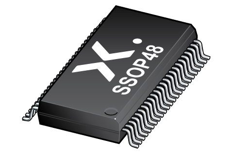
| 74ALVC164245DL | SSOP48 |
PCB Symbol, Footprint and 3D Model
| Model Name | 描述 |
|---|---|
|
|
封装
下表中的所有产品型号均已停产 。
| 型号 | 可订购的器件编号,(订购码(12NC)) | 状态 | 标示 | 封装 | 外形图 | 回流焊/波峰焊 | 包装 |
|---|---|---|---|---|---|---|---|
| 74ALVC164245DL | 74ALVC164245DL,118 (935202340118) |
Withdrawn / End-of-life | ALVC164245 |

SSOP48 (SOT370-1) |
SOT370-1 |
SSOP-TSSOP-VSO-REFLOW
SSOP-TSSOP-VSO-WAVE |
SOT370-1_118 |
| 74ALVC164245DL,112 (935202340112) |
Obsolete | ALVC164245 | 暂无信息 |
环境信息
下表中的所有产品型号均已停产 。
| 型号 | 可订购的器件编号 | 化学成分 | RoHS | RHF指示符 |
|---|---|---|---|---|
| 74ALVC164245DL | 74ALVC164245DL,118 | 74ALVC164245DL |
|
|
| 74ALVC164245DL | 74ALVC164245DL,112 | 74ALVC164245DL |
|
|
Series
文档 (8)
| 文件名称 | 标题 | 类型 | 日期 |
|---|---|---|---|
| 74ALVC164245 | 16-bit dual supply translating transceiver; 3-state | Data sheet | 2024-04-24 |
| AN90063 | Questions about package outline drawings | Application note | 2025-03-12 |
| Nexperia_document_guide_Logic_translators | Nexperia Logic Translators | Brochure | 2021-04-12 |
| alvc164245 | alvc164245 IBIS model | IBIS model | 2013-04-08 |
| Nexperia_package_poster | Nexperia package poster | Leaflet | 2020-05-15 |
| SOT370-1 | plastic, shrink small outline package; 48 leads; 0.635 mm pitch; 15.9 mm x 7.5 mm x 2.8 mm body | Package information | 2020-04-21 |
| SSOP-TSSOP-VSO-REFLOW | Footprint for reflow soldering | Reflow soldering | 2009-10-08 |
| SSOP-TSSOP-VSO-WAVE | Footprint for wave soldering | Wave soldering | 2009-10-08 |
Longevity
The Nexperia Longevity Program is aimed to provide our customers information from time to time about the expected time that our products can be ordered. The NLP is reviewed and updated regularly by our Executive Management Team. View our longevity program here.
模型
| 文件名称 | 标题 | 类型 | 日期 |
|---|---|---|---|
| alvc164245 | alvc164245 IBIS model | IBIS model | 2013-04-08 |
PCB Symbol, Footprint and 3D Model
| Model Name | 描述 |
|---|---|
|
|
How does it work?
The interactive datasheets are based on the Nexperia MOSFET precision electrothermal models. With our interactive datasheets you can simply specify your own conditions interactively. Start by changing the values of the conditions. You can do this by using the sliders in the condition fields. By dragging the sliders you will see how the MOSFET will perform at the new conditions set.
