Register once, drag and drop ECAD models into your CAD tool and speed up your design.
Click here for more information74LV595DB
8-bit serial-in/serial-out or parallel-out shift register; 3-state
The 74LV595 is an 8-bit serial-in/serial or parallel-out shift register with a storage register and 3-state outputs. Both the shift and storage register have separate clocks. The device features a serial input (DS) and a serial output (Q7S) to enable cascading and an asynchronous reset MR input. A LOW on MR will reset the shift register. Data is shifted on the LOW-to-HIGH transitions of the SHCP input. The data in the shift register is transferred to the storage register on a LOW-to-HIGH transition of the STCP input. If both clocks are connected together, the shift register will always be one clock pulse ahead of the storage register. Data in the storage register appears at the output whenever the output enable input (OE) is LOW. A HIGH on OE causes the outputs to assume a high-impedance OFF-state. Operation of the OE input does not affect the state of the registers. Inputs include clamp diodes. This enables the use of current limiting resistors to interface inputs to voltages in excess VCC.
Alternatives
Features and benefits
Wide supply voltage range from 1.0 V to 3.6 V
CMOS low power dissipation
Direct interface with TTL levels
Typical output ground bounce < 0.8 V at VCC = 3.3 V and Tamb = 25 °C
Typical HIGH-level output voltage (VOH) undershoot: > 2 V at VCC = 3.3 V and Tamb = 25 °C
Has a shift register with direct clear
Output capability:
Parallel outputs; bus driver
Serial output; standard
Latch-up performance exceeds 100 mA per JESD 78 Class II Level B
Complies with JEDEC standards
JESD8-7 (1.65 V to 1.95 V)
JESD8-5 (2.3 V to 2.7 V)
JESD8C (2.7 V to 3.6 V)
ESD protection:
HBM: ANSI/ESDA/JEDEC JS-001 class 2 exceeds 2000 V
CDM: ANSI/ESDA/JEDEC JS-002 class C3 exceeds 1000 V
Multiple package options
Specified from -40 °C to 85 °C and -40 °C to 125 °C
Applications
Serial-to-parallel data conversion
Remote control holding register
参数类型
| 型号 | Package name |
|---|---|
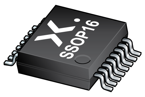
| 74LV595DB | SSOP16 |
PCB Symbol, Footprint and 3D Model
| Model Name | 描述 |
|---|---|
|
|
封装
下表中的所有产品型号均已停产 。
| 型号 | 可订购的器件编号,(订购码(12NC)) | 状态 | 标示 | 封装 | 外形图 | 回流焊/波峰焊 | 包装 |
|---|---|---|---|---|---|---|---|
| 74LV595DB | 74LV595DB,112 (935198280112) |
Obsolete | LV595 |

SSOP16 (SOT338-1) |
SOT338-1 |
SSOP-TSSOP-VSO-REFLOW
SSOP-TSSOP-VSO-WAVE |
暂无信息 |
| 74LV595DB,118 (935198280118) |
Obsolete | LV595 | 暂无信息 |
文档 (8)
| 文件名称 | 标题 | 类型 | 日期 |
|---|---|---|---|
| 74LV595 | 8-bit serial-in/serial-out or parallel-out shift register; 3-state | Data sheet | 2024-04-08 |
| lv595 | 74LV595 IBIS model | IBIS model | 2019-02-04 |
| Nexperia_package_poster | Nexperia package poster | Leaflet | 2020-05-15 |
| SSOP16_SOT338-1_mk | plastic, shrink small outline package; 16 leads; 0.65 mm pitch; 6.2 mm x 5.3 mm x 2 mm body | Marcom graphics | 2017-01-28 |
| SOT338-1 | plastic, shrink small outline package; 16 leads; 0.65 mm pitch; 6.2 mm x 5.3 mm x 2 mm body | Package information | 2022-06-20 |
| SSOP-TSSOP-VSO-REFLOW | Footprint for reflow soldering | Reflow soldering | 2009-10-08 |
| lv | lv Spice model | SPICE model | 2013-05-07 |
| SSOP-TSSOP-VSO-WAVE | Footprint for wave soldering | Wave soldering | 2009-10-08 |
Longevity
The Nexperia Longevity Program is aimed to provide our customers information from time to time about the expected time that our products can be ordered. The NLP is reviewed and updated regularly by our Executive Management Team. View our longevity program here.
PCB Symbol, Footprint and 3D Model
| Model Name | 描述 |
|---|---|
|
|
How does it work?
The interactive datasheets are based on the Nexperia MOSFET precision electrothermal models. With our interactive datasheets you can simply specify your own conditions interactively. Start by changing the values of the conditions. You can do this by using the sliders in the condition fields. By dragging the sliders you will see how the MOSFET will perform at the new conditions set.
