可订购部件
| 型号 | 可订购的器件编号 | 订购代码(12NC) | 封装 | 从经销商处购买 |
|---|---|---|---|---|
| NID1100GV | NID1100GVH | 935691826125 | SOT753 | 订单产品 |
试用我们种类齐全的评估板,体验我们的设备及其性能。深入了解我们的产品如何助您提高效率、稳健性和可靠性,让您的应用大受裨益。您可以在这里找到聚焦在应用、封装和不同的 Nexperia 产品的评估板。

Register once, drag and drop ECAD models into your CAD tool and speed up your design.
Click here for more information1.5 V to 5.5 V, 1 A, ideal diode with forward voltage blocking
The NID1100 is a low forward-voltage drop ideal diode with forward and reverse voltage blocking. It can be used to replace rectifiers in low voltage systems unable to tolerate the high voltage drops of conventional Schottky diodes. The device operates over an input voltage range of 1.5 V to 5.5 V and can support up to 1 A continuous current. They can also be used in dual supply systems in an OR-ing configuration to switch the load seamlessly from one supply to the next.
The EN pin determines the operation mode of the NID1100. When EN is low, the NID1100 blocks voltages in both forward and reverse directions. When the enable input goes high, and the input voltage is higher than the output voltage, the NID1100 starts up in controlled manner limiting the inrush current. Once inrush is complete, the device regulates the voltage between the IN and OUT pins resulting in a forward voltage drop, VFWD, approximately an order of magnitude smaller than similarly rated Schottky diodes. If at any time, the OUT voltage becomes higher than IN voltage, the NID1100 stops conducting with very low leakage currents.
NID1100 also includes short circuit current limiting and over temperature shut down to provide robust protection against load fault conditions. The open-drain ST pin can be used to monitor the status of the NID1100. The ST pin pulls low when the device is disabled, in reverse voltage blocking state or in over temperature shut down.
A variety of power OR-ing configurations are supported for system flexibility:
Two, or more, NID1100 devices
NID1100s and conventional Schottky diodes
NID1100 and an external PMOS
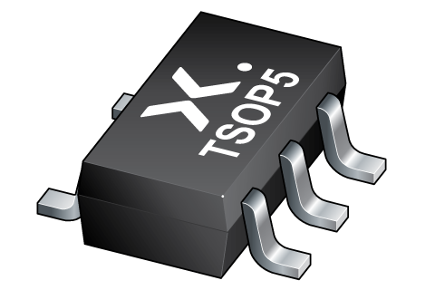
The NID1100 is available in a standard SOT753 (SC-74A) package and is characterized for operation over a junction temperature range of –40 °C to 125 °C.
Low forward drop voltage: VFWD = 120 mV (typ. at 3.6 V input and 1 A load current)
Reverse voltage blocking always
Forward voltage blocking when disabled
Low quiescent current
Enhanced load transient response
Controlled rise time at start-up
Over temperature protection
Short circuit protection
Specified over Tj= -40 °C to +125 °C
IoT systems
Gas meters, smart meters
CO Detectors
Battery backup systems
USB powered devices

| 型号 | 可订购的器件编号,(订购码(12NC)) | 状态 | 标示 | 封装 | 外形图 | 回流焊/波峰焊 | 包装 |
|---|---|---|---|---|---|---|---|
| NID1100GV | NID1100GVH (935691826125) |
Active | u2 |

TSOP5 (SOT753) |
SOT753 |
REFLOW_BG-BD-1
WAVE_BG-BD-1 |
SOT753_125 |
| Part number | Description | Type | Quick links | Shop link |
|---|---|---|---|---|
|
描述 The NEVB-NID1100 evaluation board is a two-layer PCB equipped with two NID1100 ideal diodes and one PMOS transistor. It allows users to explore the device's behavior under various application conditions.
|
类型 Evaluation board
|
Quick links
|
Shop link
|
| 文件名称 | 标题 | 类型 | 日期 |
|---|---|---|---|
| NID1100 | 1.5 V to 5.5 V, 1 A, ideal diode with forward voltage blocking | Data sheet | 2025-03-17 |
| Nexperia_document_guide_MiniLogic_PicoGate_201901 | PicoGate leaded logic portfolio guide | Brochure | 2019-01-07 |
| SOT753 | 3D model for products with SOT753 package | Design support | 2019-01-22 |
| Nexperia_package_poster | Nexperia package poster | Leaflet | 2020-05-15 |
| SOT753 | plastic, surface-mounted package; 5 leads; 0.95 mm pitch; 2.9 mm x 1.5 mm x 1 mm body | Package information | 2022-05-31 |
| SOT753_125 | TSOP5; Reel pack for SMD, 7"; Q3/T4 product orientation | Packing information | 2020-04-21 |
| REFLOW_BG-BD-1 | Reflow soldering profile | Reflow soldering | 2021-04-06 |
| aaa-042075 | NID1100 | Test circuit | 2025-01-17 |
| MAR_SOT753 | MAR_SOT753 Topmark | Top marking | 2013-06-03 |
| UM90044 | NID1100, 1.5 V to 5.5 V, 1 A, ideal diode with forward voltage blocking evaluation board | User manual | 2025-01-17 |
| WAVE_BG-BD-1 | Wave soldering profile | Wave soldering | 2021-09-08 |
The Nexperia Longevity Program is aimed to provide our customers information from time to time about the expected time that our products can be ordered. The NLP is reviewed and updated regularly by our Executive Management Team. View our longevity program here.
| 文件名称 | 标题 | 类型 | 日期 |
|---|---|---|---|
| SOT753 | 3D model for products with SOT753 package | Design support | 2019-01-22 |
| 型号 | Orderable part number | Ordering code (12NC) | 状态 | 包装 | Packing Quantity | 在线购买 |
|---|---|---|---|---|---|---|
| NID1100GV | NID1100GVH | 935691826125 | Active | SOT753_125 | 3,000 |
|
作为 Nexperia 的客户,您可以通过我们的销售机构订购样品。
如果您没有 Nexperia 的直接账户,我们的全球和地区分销商网络可为您提供 Nexperia 样品支持。查看官方经销商列表。
The interactive datasheets are based on the Nexperia MOSFET precision electrothermal models. With our interactive datasheets you can simply specify your own conditions interactively. Start by changing the values of the conditions. You can do this by using the sliders in the condition fields. By dragging the sliders you will see how the MOSFET will perform at the new conditions set.