
特性
-
Wide supply voltage range:
-
VCC(A): 0.8 V to 3.6 V
-
VCC(B): 0.8 V to 3.6 V
-
-
Complies with JEDEC standards:
-
JESD8-12 (0.8 V to 1.3 V)
-
JESD8-11 (0.9 V to 1.65 V)
-
JESD8-7 (1.2 V to 1.95 V)
-
JESD8-5 (1.8 V to 2.7 V)
-
JESD8-B (2.7 V to 3.6 V)
-
-
Maximum data rates:
-
380 Mbit/s (≥ 1.8 V to 3.3 V translation)
-
200 Mbit/s (≥ 1.1 V to 3.3 V translation)
-
200 Mbit/s (≥ 1.1 V to 2.5 V translation)
-
200 Mbit/s (≥ 1.1 V to 1.8 V translation)
-
150 Mbit/s (≥ 1.1 V to 1.5 V translation)
-
100 Mbit/s (≥ 1.1 V to 1.2 V translation)
-
-
Latch-up performance exceeds 100 mA per JESD 78 Class II
-
Inputs accept voltages up to 3.6 V
-
ESD protection:
-
HBM: ANSI/ESDA/JEDEC JS-001 class 2 exceeds 2000 V
-
CDM: ANSI/ESDA/JEDEC JS-002 class C3 exceeds 1000 V
-
-
Specified from -40 °C to +85 °C and -40 °C to +125 °C
参数类型
| Type number | Product status | VCC(A) (V) | VCC(B) (V) | Logic switching levels | Output drive capability (mA) | tpd (ns) | Nr of bits | Power dissipation considerations | Tamb (°C) | Rth(j-a) (K/W) | Ψth(j-top) (K/W) | Rth(j-c) (K/W) | Package name | Category |
|---|---|---|---|---|---|---|---|---|---|---|---|---|---|---|
| 74AVC1T1004DP | Production | 0.8 - 3.6 | 0.8 - 3.6 | CMOS/LVTTL | ± 12 | 4.9 | 1 | very low | -40~125 | 188 | 23.9 | 96.8 | TSSOP10 | Uni-directional |
封装
| 型号 | 封装 | 尺寸版本 | 回流焊/波峰焊 | 包装 | 状态 | 标示 | 可订购的器件编号,(订购码(12NC)) |
|---|---|---|---|---|---|---|---|
| 74AVC1T1004DP | 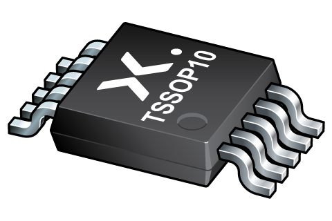 TSSOP10 (SOT552-1) | SOT552-1 | SSOP-TSSOP-VSO-WAVE | SOT552-1_118 | Active | Bc | 74AVC1T1004DPJ ( 9356 901 22118 ) |
文档 (5)
| 文件名称 | 标题 | 类型 | 日期 |
|---|---|---|---|
| 74AVC1T1004 | 1-to-4 fan-out buffer | Data sheet | 2024-06-25 |
| avc1t1004 | 74AVC1T1004 IBIS model | IBIS model | 2018-06-18 |
| Nexperia_Selection_guide_2023 | Nexperia Selection Guide 2023 | Selection guide | 2023-05-10 |
| SSOP-TSSOP-VSO-WAVE | Footprint for wave soldering | Wave soldering | 2009-10-08 |
| SOT552-1 | plastic, thin shrink small outline package; 10 leads; 0.5 mm pitch; 3 mm x 3 mm x 1.1 mm body | Package information | 2022-06-07 |
支持
如果您需要设计/技术支持,请告知我们并填写 应答表, 我们会尽快回复您。
模型
| 文件名称 | 标题 | 类型 | 日期 |
|---|---|---|---|
| avc1t1004 | 74AVC1T1004 IBIS model | IBIS model | 2018-06-18 |
订购、定价与供货
样品
作为 Nexperia 的客户,您可以通过我们的销售机构订购样品。
如果您没有 Nexperia 的直接账户,我们的全球和地区分销商网络可为您提供 Nexperia 样品支持。查看官方 经销商列表。