
特性
-
Automotive product qualification in accordance with AEC-Q100 (Grade 1)
-
Specified from -40 °C to +85 °C and from -40 °C to +125 °C
-
-
Wide supply voltage range from 1.65 V to 5.5 V
-
Overvoltage tolerant inputs to 5.5 V
-
High noise immunity
-
±24 mA output drive (VCC = 3.0 V)
-
CMOS low power dissipation
-
Latch-up performance exceeds 250 mA
-
Direct interface with TTL levels
- IOFF circuitry provides partial Power-down mode operation
-
Complies with JEDEC standard:
-
JESD8-7 (1.65 V to 1.95 V)
-
JESD8-5 (2.3 V to 2.7 V)
-
JESD8C (2.7 V to 3.6 V)
-
JESD36 (4.5 V to 5.5 V)
-
-
ESD protection:
-
HBM: ANSI/ESDA/JEDEC JS-001 class 2 exceeds 2000 V
-
CDM: ANSI/ESDA/JEDEC JS-002 class C3 exceeds 1000 V
-
参数类型
| Type number | Product status | VCC (V) | Logic switching levels | Output drive capability (mA) | tpd (ns) | Power dissipation considerations | Tamb (°C) | Rth(j-a) (K/W) | Ψth(j-top) (K/W) | Rth(j-c) (K/W) | Package name |
|---|---|---|---|---|---|---|---|---|---|---|---|
| 74LVC1G19GW-Q100 | Production | 1.65 - 5.5 | CMOS/LVTTL | ± 32 | 1.8 | low | -40~125 | 282 | 54.1 | 169 | TSSOP6 |
封装
| 型号 | 封装 | 尺寸版本 | 回流焊/波峰焊 | 包装 | 状态 | 标示 | 可订购的器件编号,(订购码(12NC)) |
|---|---|---|---|---|---|---|---|
| 74LVC1G19GW-Q100 | 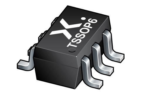 TSSOP6 (SOT363-2) | SOT363-2 | SOT363-2_125 | Active | VY | 74LVC1G19GW-Q100H ( 9353 073 07125 ) |
环境信息
| 型号 | 可订购的器件编号 | 化学成分 | RoHS | RHF指示符 | 无铅转换日期 |
|---|---|---|---|---|---|
| 74LVC1G19GW-Q100 | 74LVC1G19GW-Q100H | 74LVC1G19GW-Q100 | Always Pb-free |
文档 (6)
| 文件名称 | 标题 | 类型 | 日期 |
|---|---|---|---|
| 74LVC1G19_Q100 | 1-of-2 decoder/demultiplexer | Data sheet | 2023-08-16 |
| AN10161 | PicoGate Logic footprints | Application note | 2002-10-29 |
| AN11009 | Pin FMEA for LVC family | Application note | 2019-01-09 |
| lvc1g19 | 74LVC1G19 IBIS model | IBIS model | 2014-10-20 |
| Nexperia_Selection_guide_2023 | Nexperia Selection Guide 2023 | Selection guide | 2023-05-10 |
| SOT363-2 | plastic thin shrink small outline package; 6 leads; body width 1.25 mm | Package information | 2022-11-21 |
订购、定价与供货
样品
作为 Nexperia 的客户,您可以通过我们的销售机构订购样品。
如果您没有 Nexperia 的直接账户,我们的全球和地区分销商网络可为您提供 Nexperia 样品支持。查看官方 经销商列表。