
特性
-
Automotive product qualification in accordance with AEC-Q100 (Grade 1)
-
Specified from -40 °C to +85 °C and from -40 °C to +125 °C
-
-
Wide supply voltage range from 1.2 V to 3.6 V
-
Overvoltage tolerant inputs to 5.5 V
-
CMOS low power dissipation
-
Direct interface with TTL levels
-
IOFF circuitry provides partial Power-down mode operation
-
8-bit positive edge-triggered register
-
Independent register and 3-state buffer operation
-
Complies with JEDEC standard:
-
JESD8-7A (1.65 V to 1.95 V)
-
JESD8-5A (2.3 V to 2.7 V)
-
JESD8-C/JESD36 (2.7 V to 3.6 V)
-
-
ESD protection:
-
HBM: ANSI/ESDA/JEDEC JS-001 class 2 exceeds 2000 V
-
CDM: ANSI/ESDA/JEDEC JS-002 class C3 exceeds 1000 V
-
-
DHVQFN package with Side-Wettable Flanks enabling Automatic Optical Inspection (AOI) of solder joints
参数类型
| Type number | Product status | VCC (V) | Logic switching levels | Output drive capability (mA) | tpd (ns) | fmax (MHz) | Power dissipation considerations | Tamb (°C) | Rth(j-a) (K/W) | Ψth(j-top) (K/W) | Rth(j-c) (K/W) | Package name |
|---|---|---|---|---|---|---|---|---|---|---|---|---|
| 74LVC374ABQ-Q100 | Production | 1.2 - 3.6 | CMOS/LVTTL | ± 24 | 2.7 | 100 | low | -40~125 | 78 | 9.0 | 49 | DHVQFN20 |
| 74LVC374AD-Q100 | Production | 1.2 - 3.6 | CMOS/LVTTL | ± 24 | 2.7 | 100 | low | -40~125 | 85 | 27.1 | 61 | SO20 |
| 74LVC374APW-Q100 | Production | 1.2 - 3.6 | CMOS/LVTTL | ± 24 | 2.7 | 100 | low | -40~125 | 101 | 4.6 | 45 | TSSOP20 |
封装
| 型号 | 封装 | 尺寸版本 | 回流焊/波峰焊 | 包装 | 状态 | 标示 | 可订购的器件编号,(订购码(12NC)) |
|---|---|---|---|---|---|---|---|
| 74LVC374ABQ-Q100 | 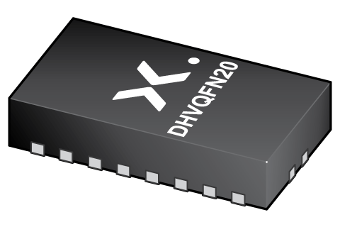 DHVQFN20 (SOT764-1) | SOT764-1 | SOT764-1_115 | Active | LVC374A | 74LVC374ABQ-Q100X ( 9352 993 15115 ) | |
| 74LVC374AD-Q100 | 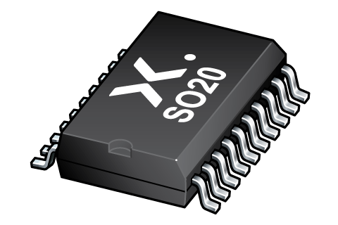 SO20 (SOT163-1) | SOT163-1 | WAVE_BG-BD-1 | SOT163-1_118 | Active | 74LVC374AD | 74LVC374AD-Q100J ( 9352 993 16118 ) |
| 74LVC374APW-Q100 | 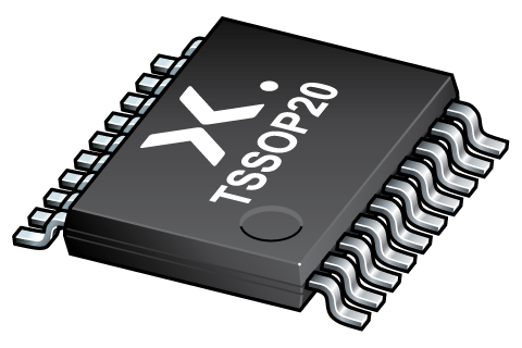 TSSOP20 (SOT360-1) | SOT360-1 | SSOP-TSSOP-VSO-WAVE | SOT360-1_118 | Active | LVC374A | 74LVC374APW-Q100J ( 9352 993 17118 ) |
环境信息
| 型号 | 可订购的器件编号 | 化学成分 | RoHS | RHF指示符 | 无铅转换日期 |
|---|---|---|---|---|---|
| 74LVC374ABQ-Q100 | 74LVC374ABQ-Q100X | 74LVC374ABQ-Q100 | Always Pb-free | ||
| 74LVC374AD-Q100 | 74LVC374AD-Q100J | 74LVC374AD-Q100 | Always Pb-free | ||
| 74LVC374APW-Q100 | 74LVC374APW-Q100J | 74LVC374APW-Q100 | Always Pb-free |
文档 (11)
| 文件名称 | 标题 | 类型 | 日期 |
|---|---|---|---|
| 74LVC374A_Q100 | Octal D-type flip-flop; 5 V tolerant inputs/outputs; positive-edge trigger; 3-state | Data sheet | 2023-09-01 |
| AN263 | Power considerations when using CMOS and BiCMOS logic devices | Application note | 2023-02-07 |
| AN11009 | Pin FMEA for LVC family | Application note | 2019-01-09 |
| lvc374a | lvc374a IBIS model | IBIS model | 2013-04-07 |
| Nexperia_Selection_guide_2023 | Nexperia Selection Guide 2023 | Selection guide | 2023-05-10 |
| lvc | lvc Spice model | SPICE model | 2013-05-06 |
| SOT764-1 | plastic, leadless dual in-line compatible thermal enhanced very thin quad flat package; 20 terminals; 0.5 mm pitch; 4.5 mm x 2.5 mm x 1 mm body | Package information | 2022-06-21 |
| SSOP-TSSOP-VSO-WAVE | Footprint for wave soldering | Wave soldering | 2009-10-08 |
| SOT360-1 | plastic, thin shrink small outline package; 20 leads; 0.65 mm pitch; 6.5 mm x 4.4 mm x 1.1 mm body | Package information | 2022-06-21 |
| SOT163-1 | plastic, small outline package; 20 leads; 1.27 mm pitch; 12.8 mm x 7.5 mm x 2.65 mm body | Package information | 2022-06-20 |
| WAVE_BG-BD-1 | Wave soldering profile | Wave soldering | 2021-09-08 |
支持
如果您需要设计/技术支持,请告知我们并填写 应答表, 我们会尽快回复您。
样品
作为 Nexperia 的客户,您可以通过我们的销售机构订购样品。
如果您没有 Nexperia 的直接账户,我们的全球和地区分销商网络可为您提供 Nexperia 样品支持。查看官方 经销商列表。