
参数类型
| 型号 | VCC(A) (V) | VCC(B) (V) | Logic switching levels | Output drive capability (mA) | tpd (ns) | Nr of bits | Power dissipation considerations | Tamb (°C) | Rth(j-a) (K/W) | Ψth(j-top) (K/W) | Rth(j-c) (K/W) | Package name | Category |
|---|---|---|---|---|---|---|---|---|---|---|---|---|---|
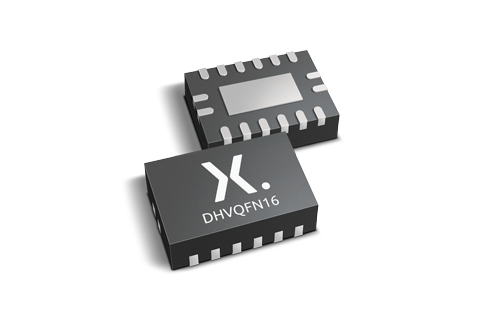
| 74AVCH4T245BQ | 0.8 - 3.6 | 0.8 - 3.6 | CMOS/LVTTL | ± 12 | 2.1 | 4 | very low | -40~125 | 92 | 13.1 | 61 | DHVQFN16 | Bi-directional | Direction controlled |
| 74AVCH4T245BQ-Q100 | 0.8 - 3.6 | 0.8 - 3.6 | CMOS/LVTTL | ± 12 | 2.1 | 4 | very low | -40~125 | 92 | 13.1 | 61 | DHVQFN16 | |
| 74AVCH4T245D | 0.8 - 3.6 | 0.8 - 3.6 | CMOS/LVTTL | ± 12 | 2.1 | 4 | very low | -40~125 | 92 | 9.2 | 51 | SO16 | Bi-directional | Direction controlled |
| 74AVCH4T245D-Q100 | 0.8 - 3.6 | 0.8 - 3.6 | CMOS/LVTTL | ± 12 | 2.1 | 4 | very low | -40~125 | 92 | 9.2 | 51 | SO16 | |
| 74AVCH4T245GU | 0.8 - 3.6 | 0.8 - 3.6 | CMOS/LVTTL | ± 12 | 2.1 | 4 | very low | -40~125 | 99 | 4.1 | 88 | XQFN16 | Bi-directional | Direction controlled |
| 74AVCH4T245PW | 0.8 - 3.6 | 0.8 - 3.6 | CMOS/LVTTL | ± 12 | 2.1 | 4 | very low | -40~125 | 124 | 4.4 | 53.6 | TSSOP16 | Bi-directional | Direction controlled |
| 74AVCH4T245PW-Q100 | 0.8 - 3.6 | 0.8 - 3.6 | CMOS/LVTTL | ± 12 | 2.1 | 4 | very low | -40~125 | 124 | 4.4 | 53.6 | TSSOP16 |
封装
| 型号 | 可订购的器件编号,(订购码(12NC)) | 状态 | 标示 | 封装 | 外形图 | 回流焊/波峰焊 | 包装 |
|---|---|---|---|---|---|---|---|
| 74AVCH4T245BQ | 74AVCH4T245BQ,115 (935284587115) |
Active | H4T245 |
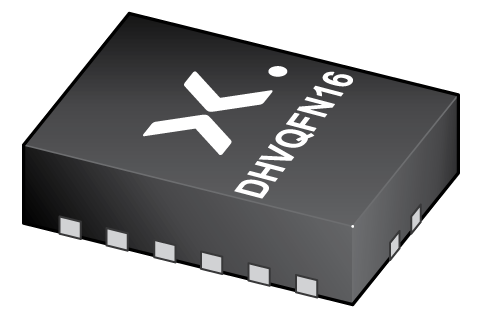
DHVQFN16 (SOT763-1) |
SOT763-1 | SOT763-1_115 | |
| 74AVCH4T245BQ-Q100 | 74AVCH4T245BQ-Q10X (935302455115) |
Active | H4T245 |
DHVQFN16 (SOT763-1) |
SOT763-1 | SOT763-1_115 | |
| 74AVCH4T245D | 74AVCH4T245D,118 (935288132118) |
Active | 74AVCH4T245D |
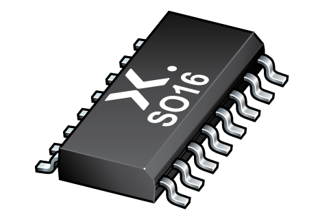
SO16 (SOT109-1) |
SOT109-1 |
SO-SOJ-REFLOW
SO-SOJ-WAVE WAVE_BG-BD-1 |
SOT109-1_118 |
| 74AVCH4T245D-Q100 | 74AVCH4T245D-Q100J (935302456118) |
Active | 74AVCH4T245D |
SO16 (SOT109-1) |
SOT109-1 |
SO-SOJ-REFLOW
SO-SOJ-WAVE WAVE_BG-BD-1 |
SOT109-1_118 |
| 74AVCH4T245GU | 74AVCH4T245GU,115 (935293386115) |
Active | K4 |
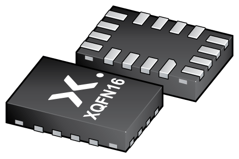
XQFN16 (SOT1161-1) |
SOT1161-1 | SOT1161-1_115 | |
| 74AVCH4T245PW | 74AVCH4T245PW,118 (935284589118) |
Active | CH4T245 |
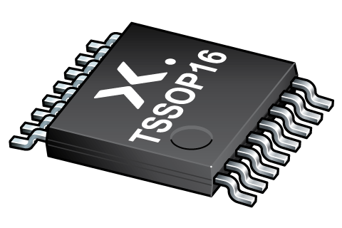
TSSOP16 (SOT403-1) |
SOT403-1 |
SSOP-TSSOP-VSO-WAVE
|
SOT403-1_118 |
| 74AVCH4T245PW-Q100 | 74AVCH4T245PW-Q10J (935302458118) |
Active | CH4T245 |
TSSOP16 (SOT403-1) |
SOT403-1 |
SSOP-TSSOP-VSO-WAVE
|
SOT403-1_118 |
环境信息
| 型号 | 可订购的器件编号 | 化学成分 | RoHS | RHF指示符 |
|---|---|---|---|---|
| 74AVCH4T245BQ | 74AVCH4T245BQ,115 | 74AVCH4T245BQ |
|
|
| 74AVCH4T245BQ-Q100 | 74AVCH4T245BQ-Q10X | 74AVCH4T245BQ-Q100 |
|
|
| 74AVCH4T245D | 74AVCH4T245D,118 | 74AVCH4T245D |
|
|
| 74AVCH4T245D-Q100 | 74AVCH4T245D-Q100J | 74AVCH4T245D-Q100 |
|
|
| 74AVCH4T245GU | 74AVCH4T245GU,115 | 74AVCH4T245GU |
|
|
| 74AVCH4T245PW | 74AVCH4T245PW,118 | 74AVCH4T245PW |
|
|
| 74AVCH4T245PW-Q100 | 74AVCH4T245PW-Q10J | 74AVCH4T245PW-Q100 |
|
|
文档 (21)
| 文件名称 | 标题 | 类型 | 日期 |
|---|---|---|---|
| 74AVCH4T245 | 4-bit dual supply translating transceiver with configurable voltage translation; 3-state | Data sheet | 2024-04-11 |
| AN90063 | Questions about package outline drawings | Application note | 2025-03-12 |
| Nexperia_document_guide_Logic_translators | Nexperia Logic Translators | Brochure | 2021-04-12 |
| SOT763-1 | 3D model for products with SOT763-1 package | Design support | 2019-10-03 |
| SOT109-1 | 3D model for products with SOT109-1 package | Design support | 2020-01-22 |
| SOT1161-1 | 3D model for products with SOT1161-1 package | Design support | 2023-02-07 |
| SOT403-1 | 3D model for products with SOT403-1 package | Design support | 2020-01-22 |
| avch4t245 | 74AVCH4T245 IBIS model | IBIS model | 2019-01-09 |
| Nexperia_package_poster | Nexperia package poster | Leaflet | 2020-05-15 |
| DHVQFN16_SOT763-1_mk | plastic, dual in-line compatible thermal enhanced very thin quad flat package; 16 terminals; 0.5 mm pitch; 3.5 mm x 2.5 mm x 0.85 mm body | Marcom graphics | 2017-01-28 |
| SO16_SOT109-1_mk | plastic, small outline package; 16 leads; 1.27 mm pitch; 9.9 mm x 3.9 mm x 1.35 mm body | Marcom graphics | 2017-01-28 |
| TSSOP16_SOT403-1_mk | plastic, thin shrink small outline package; 16 leads; 0.65 mm pitch; 5 mm x 4.4 mm x 1.1 mm body | Marcom graphics | 2017-01-28 |
| SOT763-1 | plastic, leadless dual in-line compatible thermal enhanced very thin quad flat package; 16 terminals; 0.5 mm pitch; 3.5 mm x 2.5 mm x 1 mm body | Package information | 2023-05-11 |
| SOT109-1 | plastic, small outline package; 16 leads; 1.27 mm pitch; 9.9 mm x 3.9 mm x 1.75 mm body | Package information | 2023-11-07 |
| SOT1161-1 | plastic, leadless extermely thin quad flat package; 16 terminals; 0.4 mm pitch; 2.6 mm x 1.8 mm x 0.5 mm body | Package information | 2022-06-15 |
| SOT403-1 | plastic, thin shrink small outline package; 16 leads; 5 mm x 4.4 mm x 1.2 mm body | Package information | 2023-11-08 |
| SO-SOJ-REFLOW | Footprint for reflow soldering | Reflow soldering | 2009-10-08 |
| Nexperia_Selection_guide_2023 | Nexperia Selection Guide 2023 | Selection guide | 2023-05-10 |
| SO-SOJ-WAVE | Footprint for wave soldering | Wave soldering | 2009-10-08 |
| WAVE_BG-BD-1 | Wave soldering profile | Wave soldering | 2021-09-08 |
| SSOP-TSSOP-VSO-WAVE | Footprint for wave soldering | Wave soldering | 2009-10-08 |
支持
如果您需要设计/技术支持,请告知我们并填写 应答表 我们会尽快回复您。
模型
| 文件名称 | 标题 | 类型 | 日期 |
|---|---|---|---|
| SOT763-1 | 3D model for products with SOT763-1 package | Design support | 2019-10-03 |
| SOT109-1 | 3D model for products with SOT109-1 package | Design support | 2020-01-22 |
| SOT1161-1 | 3D model for products with SOT1161-1 package | Design support | 2023-02-07 |
| SOT403-1 | 3D model for products with SOT403-1 package | Design support | 2020-01-22 |
| avch4t245 | 74AVCH4T245 IBIS model | IBIS model | 2019-01-09 |
Ordering, pricing & availability
样品
作为 Nexperia 的客户,您可以通过我们的销售机构订购样品。
如果您没有 Nexperia 的直接账户,我们的全球和地区分销商网络可为您提供 Nexperia 样品支持。查看官方经销商列表。