
参数类型
| 型号 |
|---|
封装
下表中的所有产品型号均已停产 。
| 型号 | 可订购的器件编号,(订购码(12NC)) | 状态 | 标示 | 封装 | 外形图 | 回流焊/波峰焊 | 包装 |
|---|---|---|---|---|---|---|---|
| 74LVC823ABQ | 74LVC823ABQ,118 (935275619118) |
Obsolete |
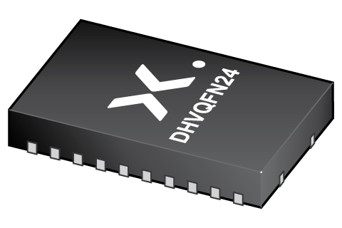
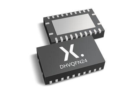
DHVQFN24 (SOT815-1) |
SOT815-1 | SOT815-1_118 | ||
| 74LVC823ABQ,115 (935275619115) |
Obsolete | 暂无信息 | |||||
| 74LVC823AD | 74LVC823AD,112 (935262539112) |
Obsolete | no package information | ||||
| 74LVC823AD,118 (935262539118) |
Obsolete | ||||||
| 74LVC823ADB | 74LVC823ADB,112 (935262540112) |
Obsolete | LVC823A Standard Procedure Standard Procedure |
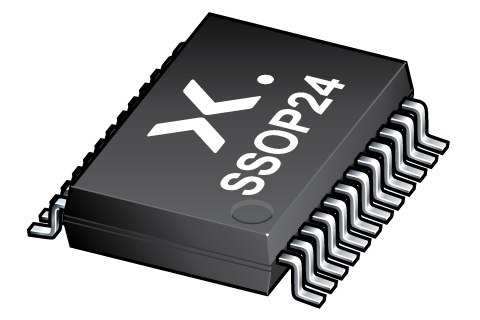
SSOP24 (SOT340-1) |
SOT340-1 |
SSOP-TSSOP-VSO-REFLOW
SSOP-TSSOP-VSO-WAVE |
暂无信息 |
| 74LVC823ADB,118 (935262540118) |
Obsolete | LVC823A Standard Procedure Standard Procedure | SOT340-1_118 | ||||
| 74LVC823APW | 74LVC823APW,112 (935262541112) |
Obsolete | LVC823A |
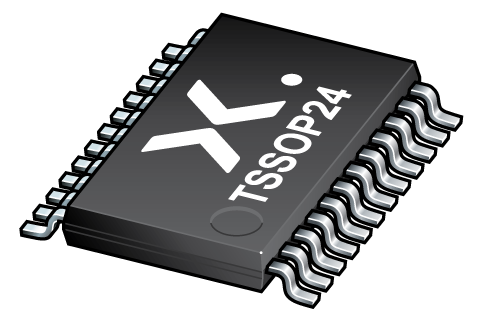
TSSOP24 (SOT355-1) |
SOT355-1 |
SSOP-TSSOP-VSO-WAVE
|
暂无信息 |
| 74LVC823APW,118 (935262541118) |
Obsolete | LVC823A | SOT355-1_118 | ||||
环境信息
下表中的所有产品型号均已停产 。
| 型号 | 可订购的器件编号 | 化学成分 | RoHS | RHF指示符 |
|---|---|---|---|---|
| 74LVC823ABQ | 74LVC823ABQ,118 | 74LVC823ABQ |
|
|
| 74LVC823ABQ | 74LVC823ABQ,115 | 74LVC823ABQ |
|
|
| 74LVC823AD | 74LVC823AD,112 | 74LVC823AD |
|
|
| 74LVC823AD | 74LVC823AD,118 | 74LVC823AD |
|
|
| 74LVC823ADB | 74LVC823ADB,112 | 74LVC823ADB |
|
|
| 74LVC823ADB | 74LVC823ADB,118 | 74LVC823ADB |
|
|
| 74LVC823APW | 74LVC823APW,112 | 74LVC823APW |
|
|
| 74LVC823APW | 74LVC823APW,118 | 74LVC823APW |
|
|
文档 (16)
| 文件名称 | 标题 | 类型 | 日期 |
|---|---|---|---|
| 74LVC823A | 9-bit D-type flip-flop with 5 V tolerant inputs/outputs; positive edge-trigger; 3-state | Data sheet | 2020-06-19 |
| AN11009 | Pin FMEA for LVC family | Application note | 2019-01-09 |
| AN263 | Power considerations when using CMOS and BiCMOS logic devices | Application note | 2023-02-07 |
| 001aaa850 | Block diagram: 74LVC823ABQ, 74LVC823AD, 74LVC823ADB, 74LVC823APW | Block diagram | 2009-11-03 |
| SOT815-1 | 3D model for products with SOT815-1 package | Design support | 2019-10-03 |
| SOT355-1 | 3D model for products with SOT355-1 package | Design support | 2020-01-22 |
| lvc823a | lvc823a IBIS model | IBIS model | 2013-04-09 |
| Nexperia_package_poster | Nexperia package poster | Leaflet | 2020-05-15 |
| DHVQFN24_SOT815-1_mk | plastic, dual in-line compatible thermal enhanced very thin quad flat package; 24 terminals; 0.5 mm pitch; 3.5 mm x 5.5 mm x 0.85 mm body | Marcom graphics | 2017-01-28 |
| SOT815-1 | plastic, leadless dual in-line compatible thermal enhanced very thin quad flat package; 24 terminals; 0.5 mm pitch; 5.5 mm x 3.5 mm x 1 mm body | Package information | 2021-08-17 |
| SOT340-1 | plastic, shrink small outline package; 24 leads; 0.65 mm pitch; 8.2 mm x 5.3 mm x 2 mm body | Package information | 2020-04-21 |
| SOT355-1 | plastic, thin shrink small outline package; 24 leads; 0.65 mm pitch; 7.8 mm x 4.4 mm x 1.2 mm body | Package information | 2024-11-15 |
| SSOP-TSSOP-VSO-REFLOW | Footprint for reflow soldering | Reflow soldering | 2009-10-08 |
| lvc | lvc Spice model | SPICE model | 2013-05-07 |
| Nexperia_Selection_guide_2023 | Nexperia Selection Guide 2023 | Selection guide | 2023-05-10 |
| SSOP-TSSOP-VSO-WAVE | Footprint for wave soldering | Wave soldering | 2009-10-08 |
支持
如果您需要设计/技术支持,请告知我们并填写 应答表 我们会尽快回复您。
Ordering, pricing & availability
样品
作为 Nexperia 的客户,您可以通过我们的销售机构订购样品。
如果您没有 Nexperia 的直接账户,我们的全球和地区分销商网络可为您提供 Nexperia 样品支持。查看官方经销商列表。