双极性晶体管

二极管

ESD保护、TVS、滤波和信号调节ESD保护

MOSFET

氮化镓场效应晶体管(GaN FET)

绝缘栅双极晶体管(IGBTs)

模拟和逻辑IC

汽车应用认证产品(AEC-Q100/Q101)

NEVB-NID1100 1.5 V to 5.5 V, 1 A, Ideal Diode with Forward Voltage Blocking Evaluation Board

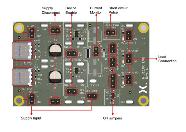
The NEVB-NID1100 evaluation board is a two-layer PCB equipped with two NID1100 ideal diodes and one PMOS transistor. It allows users to explore the device's behavior under various application conditions.

Key features & benefits

  • Input operating voltage range (VIN) 1.5 V to 5.5 V
  • Continuous output current 1 A
  • Three supply inputs VIN1, VIN2, VIN3
  • Two optional USB-C supply inputs for VIN1 and VIN2
  • Access to all device pins
  • Use case selection by means of jumpers
  • Short circuit testing

板上的产品 (1)

Type number Description Status Quick access
NID1100GV 1.5 V to 5.5 V, 1 A, ideal diode with forward voltage blocking Production

板上的产品 (1)

Type number Description Status Quick access
NID1100GV 1.5 V to 5.5 V, 1 A, ideal diode with forward voltage blocking Production

文档 (1)

文件名称 标题 类型 日期
UM90044 NID1100, 1.5 V to 5.5 V, 1 A, ideal diode with forward voltage blocking evaluation board User manual 2025-01-17