Register once, drag and drop ECAD models into your CAD tool and speed up your design.
Click here for more information74AUP2G126GD
Low-power dual buffer/line driver; 3-state
The 74AUP2G126 is a dual buffer/line driver with 3-state outputs controlled by the output enable inputs (nOE). Schmitt-trigger action at all inputs makes the circuit tolerant of slower input rise and fall times. This device ensures very low static and dynamic power consumption across the entire VCC range from 0.8 V to 3.6 V.
This device is fully specified for partial power down applications using IOFF. The IOFF circuitry disables the output, preventing the potentially damaging backflow current through the device when it is powered down.
Alternatives
Features and benefits
Wide supply voltage range from 0.8 V to 3.6 V
High noise immunity
CMOS low power dissipation
Low static power consumption; ICC = 0.9 μA (maximum)
Latch-up performance exceeds 100 mA per JESD78 Class II
Overvoltage tolerant inputs to 3.6 V
Low noise overshoot and undershoot < 10 % of VCC
Input-disable feature allows floating input conditions
IOFF circuitry provides partial Power-down mode operation
Latch-up performance exceeds 100 mA per JESD 78 Class II Level B
Complies with JEDEC standards:
JESD8-12 (0.8 V to 1.3 V)
JESD8-11 (0.9 V to 1.65 V)
JESD8-7 (1.2 V to 1.95 V)
JESD8-5 (1.8 V to 2.7 V)
JESD8C (2.7 V to 3.6 V)
ESD protection:
HBM: ANSI/ESDA/JEDEC JS-001 class 3A exceeds 5000 V
CDM: ANSI/ESDA/JEDEC JS-002 class C3 exceeds 1000 V
Multiple package options
Specified from -40 °C to +85 °C and -40 °C to +125 °C
参数类型
| 型号 | Package name |
|---|---|
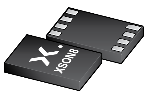
| 74AUP2G126GD | XSON8 |
封装
下表中的所有产品型号均已停产 。
| 型号 | 可订购的器件编号,(订购码(12NC)) | 状态 | 标示 | 封装 | 外形图 | 回流焊/波峰焊 | 包装 |
|---|---|---|---|---|---|---|---|
| 74AUP2G126GD | 74AUP2G126GD,125 (935288281125) |
Withdrawn / End-of-life | p26 |
XSON8 (SOT996-2) |
SOT996-2 | SOT996-2_125 |
环境信息
下表中的所有产品型号均已停产 。
| 型号 | 可订购的器件编号 | 化学成分 | RoHS | RHF指示符 |
|---|---|---|---|---|
| 74AUP2G126GD | 74AUP2G126GD,125 | 74AUP2G126GD |
|
|
Series
文档 (7)
| 文件名称 | 标题 | 类型 | 日期 |
|---|---|---|---|
| 74AUP2G126 | Low-power dual buffer/line driver; 3-state | Data sheet | 2024-05-06 |
| AN10161 | PicoGate Logic footprints | Application note | 2002-10-29 |
| AN11052 | Pin FMEA for AUP family | Application note | 2019-01-09 |
| aup2g126 | aup2g126 IBIS model | IBIS model | 2013-04-07 |
| Nexperia_document_leaflet_Logic_AUP_technology_portfolio_201904 | Nexperia_document_leaflet_Logic_AUP_technology_portfolio_201904 | Leaflet | 2019-04-12 |
| Nexperia_package_poster | Nexperia package poster | Leaflet | 2020-05-15 |
| SOT996-2 | plastic, leadless extremely thin small outline package; 8 terminals; 0.5 mm pitch; 3 mm x 2 mm x 0.5 mm body | Package information | 2020-04-21 |
Longevity
The Nexperia Longevity Program is aimed to provide our customers information from time to time about the expected time that our products can be ordered. The NLP is reviewed and updated regularly by our Executive Management Team. View our longevity program here.
模型
| 文件名称 | 标题 | 类型 | 日期 |
|---|---|---|---|
| aup2g126 | aup2g126 IBIS model | IBIS model | 2013-04-07 |
How does it work?
The interactive datasheets are based on the Nexperia MOSFET precision electrothermal models. With our interactive datasheets you can simply specify your own conditions interactively. Start by changing the values of the conditions. You can do this by using the sliders in the condition fields. By dragging the sliders you will see how the MOSFET will perform at the new conditions set.