Register once, drag and drop ECAD models into your CAD tool and speed up your design.
Click here for more information74AXP1T14GX
Dual supply Schmitt trigger inverter
The 74AXP1T14 is a dual supply Schmitt trigger inverter. It features one input (A), an output (Y) and dual supply pins (VCCI and VCCO). The input is referenced to VCCI and the output is referenced to VCCO. Input A can be connected directly to VCCI or GND. VCCI can be supplied at any voltage between 0.7 V and 2.75 V and VCCO can be supplied at any voltage between 1.2 V and 5.5 V. This feature allows voltage level translation.
This device ensures very low static and dynamic power consumption across the entire supply range and is fully specified for partial power down applications using IOFF. The IOFF circuitry disables the output, preventing the potentially damaging backflow current through the device when it is powered down.
Features and benefits
Wide supply voltage range:
VCCI: 0.7 V to 2.75 V
VCCO: 1.2 V to 5.5 V
Low input capacitance; CI = 0.6 pF (typical)
Low output capacitance; CO = 1.8 pF (typical)
Low dynamic power consumption; CPD = 0.5 pF at VCCI = 1.2 V (typical)
Low dynamic power consumption; CPD = 7.1 pF at VCCO = 3.3 V (typical)
Low static power consumption; ICCI = 0.5 μA (85 °C maximum)
Low static power consumption; ICCO = 1.8 μA (85 °C maximum)
High noise immunity
Complies with JEDEC standard:
JESD8-12A.01 (1.1 V to 1.3 V; A input)
JESD8-11A.01 (1.4 V to 1.6 V)
JESD8-7A (1.65 V to 1.95 V)
JESD8-5A.01 (2.3 V to 2.7 V)
JESD8-C (2.7 V to 3.6 V; Y output)
JESD12-6 (4.5 V to 5.5 V; Y output)
ESD protection:
HBM ANSI/ESDA/JEDEC JS-001 Class 2 exceeds 2000 V
CDM JESD22-C101E exceeds 1000 V
Latch-up performance exceeds 100 mA per JESD78D Class II
Inputs accept voltages up to 2.75 V
Low noise overshoot and undershoot < 10% of VCCO
IOFF circuitry provides partial power-down mode operation
Specified from -40 °C to +85 °C
参数类型
| 型号 | Logic switching levels | Output drive capability (mA) | Nr of bits | Power dissipation considerations | Tamb (°C) | Rth(j-a) (K/W) | Ψth(j-top) (K/W) | Rth(j-c) (K/W) | Package name |
|---|---|---|---|---|---|---|---|---|---|
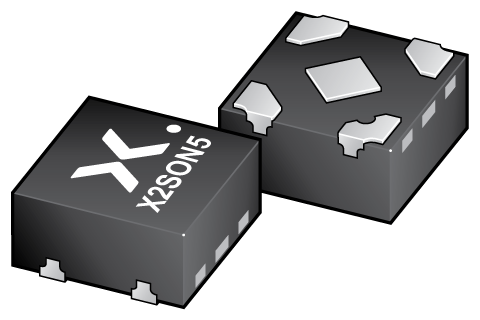
| 74AXP1T14GX | CMOS | ± 12 | 1 | ultra low | -40~85 | 306 | 76.7 | 177 | X2SON5 |
封装
下表中的所有产品型号均已停产 。
| 型号 | 可订购的器件编号,(订购码(12NC)) | 状态 | 标示 | 封装 | 外形图 | 回流焊/波峰焊 | 包装 |
|---|---|---|---|---|---|---|---|
| 74AXP1T14GX | 74AXP1T14GXH (935308975125) |
Withdrawn / End-of-life |
X2SON5 (SOT1226-3) |
SOT1226-3 | SOT1226-3_125 | ||
| 74AXP1T14GXZ (935308975147) |
Obsolete | 暂无信息 |
环境信息
下表中的所有产品型号均已停产 。
| 型号 | 可订购的器件编号 | 化学成分 | RoHS | RHF指示符 |
|---|---|---|---|---|
| 74AXP1T14GX | 74AXP1T14GXH | 74AXP1T14GX |
|
|
| 74AXP1T14GX | 74AXP1T14GXZ | 74AXP1T14GX |
|
|
文档 (9)
| 文件名称 | 标题 | 类型 | 日期 |
|---|---|---|---|
| 74AXP1T14 | Dual supply Schmitt trigger inverter | Data sheet | 2022-02-02 |
| AN90029 | Pin FMEA for AXPnT family | Application note | 2021-07-13 |
| Nexperia_document_guide_Logic_translators | Nexperia Logic Translators | Brochure | 2021-04-12 |
| SOT1226-3 | 3D model for products with SOT1226-3 package | Design support | 2021-01-28 |
| axp1t14 | 74AXP1T14 IBIS Model | IBIS model | 2016-12-13 |
| Nexperia_document_leaflet_Logic_AXP_technology_portfolio_201904 | AXP – Extremely low-power logic technology portfolio | Leaflet | 2019-04-05 |
| Nexperia_document_leaflet_Logic_X2SON_packages_062018 | X2SON ultra-small 4, 5, 6 & 8-pin leadless packages | Leaflet | 2018-06-05 |
| SOT1226-3 | plastic thermal enhanced extremely thin small outline package; no leads;5 terminals; body 0.8 x 0.8 x 0.32 mm | Package information | 2020-08-27 |
| 74AXP1T14GX_Nexperia_Product_Reliability | 74AXP1T14GX Nexperia Product Reliability | Quality document | 2025-03-20 |
Longevity
The Nexperia Longevity Program is aimed to provide our customers information from time to time about the expected time that our products can be ordered. The NLP is reviewed and updated regularly by our Executive Management Team. View our longevity program here.
How does it work?
The interactive datasheets are based on the Nexperia MOSFET precision electrothermal models. With our interactive datasheets you can simply specify your own conditions interactively. Start by changing the values of the conditions. You can do this by using the sliders in the condition fields. By dragging the sliders you will see how the MOSFET will perform at the new conditions set.