Register once, drag and drop ECAD models into your CAD tool and speed up your design.
Click here for more information74HCT573DB-Q100
Octal D-type transparent latch; 3-state
The 74HC573-Q100; 74HCT573-Q100 is an 8-bit D-type transparent latch with 3-state outputs. The device features latch enable (LE) and output enable (OE) inputs. When LE is HIGH, data at the inputs enter the latches. In this condition the latches are transparent, a latch output will change each time its corresponding D-input changes. When LE is LOW the latches store the information that was present at the inputs a set-up time preceding the HIGH-to-LOW transition of LE. A HIGH on OE causes the outputs to assume a high-impedance OFF-state. Operation of the OE input does not affect the state of the latches. Inputs include clamp diodes. This enables the use of current limiting resistors to interface inputs to voltages in excess of VCC.
This product has been qualified to the Automotive Electronics Council (AEC) standard Q100 (Grade 1) and is suitable for use in automotive applications.
Alternatives
Features and benefits
Automotive product qualification in accordance with AEC-Q100 (Grade 1)
Specified from -40 °C to +85 °C and from -40 °C to +125 °C
- Wide supply voltage range from 2.0 V to 6.0 V
- CMOS low power dissipation
- High noise immunity
Input levels:
For 74HC573-Q100: CMOS level
For 74HCT573-Q100: TTL level
Inputs and outputs on opposite sides of package allowing easy interface with microprocessors
Useful as input or output port for microprocessors and microcomputers
3-state non-inverting outputs for bus-oriented applications
Common 3-state output enable input
Multiple package options
Latch-up performance exceeds 100 mA per JESD 78 Class II Level B
Complies with JEDEC standards:
- JESD8C (2.7 V to 3.6 V)
- JESD7A (2.0 V to 6.0 V)
ESD protection:
HBM: ANSI/ESDA/JEDEC JS-001 class 2 exceeds 2000 V
CDM: ANSI/ESDA/JEDEC JS-002 class C3 exceeds 1000 V
DHVQFN package with Side-Wettable Flanks enabling Automated Optical Inspection (AOI) of solder joints
参数类型
| 型号 | Package name |
|---|---|
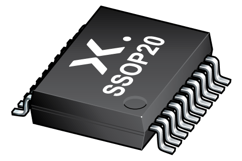
| 74HCT573DB-Q100 | SSOP20 |
封装
下表中的所有产品型号均已停产 。
| 型号 | 可订购的器件编号,(订购码(12NC)) | 状态 | 标示 | 封装 | 外形图 | 回流焊/波峰焊 | 包装 |
|---|---|---|---|---|---|---|---|
| 74HCT573DB-Q100 | 74HCT573DB-Q100J (935301414118) |
Obsolete | HCT573 |

SSOP20 (SOT339-1) |
SOT339-1 |
SSOP-TSSOP-VSO-WAVE
|
SOT339-1_118 |
Series
文档 (8)
| 文件名称 | 标题 | 类型 | 日期 |
|---|---|---|---|
| 74HC_HCT573_Q100 | Octal D-type transparent latch; 3-state | Data sheet | 2024-08-05 |
| AN11044 | Pin FMEA 74HC/74HCT family | Application note | 2019-01-09 |
| AN90063 | Questions about package outline drawings | Application note | 2025-03-12 |
| hct573 | 74HCT573 IBIS model | IBIS model | 2020-12-08 |
| Nexperia_package_poster | Nexperia package poster | Leaflet | 2020-05-15 |
| SOT339-1 | plastic, shrink small outline package; 20 leads; 0.65 mm pitch; 7.2 mm x 5.3 mm x 2 mm body | Package information | 2020-04-21 |
| HCT_USER_GUIDE | HC/T User Guide | User manual | 1997-10-31 |
| SSOP-TSSOP-VSO-WAVE | Footprint for wave soldering | Wave soldering | 2009-10-08 |
Longevity
The Nexperia Longevity Program is aimed to provide our customers information from time to time about the expected time that our products can be ordered. The NLP is reviewed and updated regularly by our Executive Management Team. View our longevity program here.
模型
| 文件名称 | 标题 | 类型 | 日期 |
|---|---|---|---|
| hct573 | 74HCT573 IBIS model | IBIS model | 2020-12-08 |
How does it work?
The interactive datasheets are based on the Nexperia MOSFET precision electrothermal models. With our interactive datasheets you can simply specify your own conditions interactively. Start by changing the values of the conditions. You can do this by using the sliders in the condition fields. By dragging the sliders you will see how the MOSFET will perform at the new conditions set.
