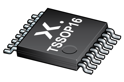
可订购部件
| 型号 | 可订购的器件编号 | 订购代码(12NC) | 封装 | 从经销商处购买 |
|---|---|---|---|---|
| HEF40175BTT | HEF40175BTT,118 | 935294421118 | SOT403-1 | 订单产品 |
试用我们种类齐全的评估板,体验我们的设备及其性能。深入了解我们的产品如何助您提高效率、稳健性和可靠性,让您的应用大受裨益。您可以在这里找到聚焦在应用、封装和不同的 Nexperia 产品的评估板。

Register once, drag and drop ECAD models into your CAD tool and speed up your design.
Click here for more informationQuad D-type flip-flop
The HEF40175B is a quad positive edge triggered D-type flip-flop with four data (Dn) inputs, common clock (CP) and asynchronous master reset (MR) inputs, and complementary Qn and Qn outputs. When MR is HIGH data at the D-input that meets the set-up and hold time requirements on the LOW-to-HIGH clock transition will be stored in the flip-flop and appear at the Q output. When LOW, MR resets all flip-flops (Qn = LOW, Qn = HIGH), independent of CP and Dn. Inputs include clamp diodes. This enables the use of current limiting resistors to interface inputs to voltages in excess of VDD.
Wide supply voltage range from 3.0 V to 15.0 V
CMOS low power dissipation
High noise immunity
Fully static operation
5 V, 10 V, and 15 V parametric ratings
Standardized symmetrical output characteristics
Complies with JEDEC standard JESD 13-B
HBM: ANSI/ESDA/JEDEC JS-001 class 2 exceeds 2000 V
CDM: ANSI/ESDA/JEDEC JS-002 class C3 exceeds 1000 V
Specified from -40 °C to +85°C and from -40 °C to +125 °C
Shift registers
Buffer/storage register
Pattern generator
| 型号 | VCC (V) | Logic switching levels | Output drive capability (mA) | tpd (ns) | fmax (MHz) | Power dissipation considerations | Tamb (°C) | Rth(j-a) (K/W) | Ψth(j-top) (K/W) | Rth(j-c) (K/W) | Package name |
|---|---|---|---|---|---|---|---|---|---|---|---|
| HEF40175BTT | 3.0 - 15 | CMOS | ± 2.4 | 25 | 45 | low | -40~85 | 115 | 2.2 | 43.2 | TSSOP16 |
| Model Name | 描述 |
|---|---|
|
|
| 型号 | 可订购的器件编号,(订购码(12NC)) | 状态 | 标示 | 封装 | 外形图 | 回流焊/波峰焊 | 包装 |
|---|---|---|---|---|---|---|---|
| HEF40175BTT | HEF40175BTT,118 (935294421118) |
Active | HF40175 |

TSSOP16 (SOT403-1) |
SOT403-1 |
SSOP-TSSOP-VSO-WAVE
|
SOT403-1_118 |
| 文件名称 | 标题 | 类型 | 日期 |
|---|---|---|---|
| HEF40175B | Quad D-type flip-flop | Data sheet | 2024-08-08 |
| AN11051 | Pin FMEA HEF4000 family | Application note | 2019-01-09 |
| SOT403-1 | 3D model for products with SOT403-1 package | Design support | 2020-01-22 |
| Nexperia_package_poster | Nexperia package poster | Leaflet | 2020-05-15 |
| TSSOP16_SOT403-1_mk | plastic, thin shrink small outline package; 16 leads; 0.65 mm pitch; 5 mm x 4.4 mm x 1.1 mm body | Marcom graphics | 2017-01-28 |
| SOT403-1 | plastic, thin shrink small outline package; 16 leads; 5 mm x 4.4 mm x 1.2 mm body | Package information | 2023-11-08 |
| SOT403-1_118 | TSSOP16; Reel pack for SMD, 13"; Q1/T1 product orientation | Packing information | 2020-04-21 |
| HEF40175BTT_Nexperia_Product_Reliability | HEF40175BTT Nexperia Product Reliability | Quality document | 2025-03-20 |
| SSOP-TSSOP-VSO-WAVE | Footprint for wave soldering | Wave soldering | 2009-10-08 |
The Nexperia Longevity Program is aimed to provide our customers information from time to time about the expected time that our products can be ordered. The NLP is reviewed and updated regularly by our Executive Management Team. View our longevity program here.
| 文件名称 | 标题 | 类型 | 日期 |
|---|---|---|---|
| SOT403-1 | 3D model for products with SOT403-1 package | Design support | 2020-01-22 |
| Model Name | 描述 |
|---|---|
|
|
| 型号 | Orderable part number | Ordering code (12NC) | 状态 | 包装 | Packing Quantity | 在线购买 |
|---|---|---|---|---|---|---|
| HEF40175BTT | HEF40175BTT,118 | 935294421118 | Active | SOT403-1_118 | 2,500 |
|
作为 Nexperia 的客户,您可以通过我们的销售机构订购样品。
如果您没有 Nexperia 的直接账户,我们的全球和地区分销商网络可为您提供 Nexperia 样品支持。查看官方经销商列表。
The interactive datasheets are based on the Nexperia MOSFET precision electrothermal models. With our interactive datasheets you can simply specify your own conditions interactively. Start by changing the values of the conditions. You can do this by using the sliders in the condition fields. By dragging the sliders you will see how the MOSFET will perform at the new conditions set.