Register once, drag and drop ECAD models into your CAD tool and speed up your design.
Click here for more informationNPIC6C596D
Power logic 8-bit shift register; open-drain outputs
The NPIC6C596 is an 8-bit serial-in/serial or parallel-out shift register with a storage register and open-drain outputs. Both the shift and storage register have separate clocks. The device features a serial input (DS) and a serial output (Q7S) to enable cascading and an asynchronous reset MR input. A LOW on MR resets both the shift register and storage register. Data is shifted on the LOW-to-HIGH transitions of the SHCP input. The data in the shift register is transferred to the storage register on a LOW-to-HIGH transition of the STCP input. If both clocks are connected together, the shift register is always one clock pulse ahead of the storage register. To provide additional hold time in cascaded applications, the serial output QS7 is clocked out on the falling edge of SHCP. Data in the storage register drives the gate of the output extended-drain NMOS (EDNMOS) transistor whenever the output enable input (OE) is LOW. A HIGH on OE causes the outputs to assume a high-impedance OFF-state. Operation of the OE input does not affect the state of the registers.
The open-drain outputs are 33 V/100 mA continuous current extended-drain NMOS transistors designed for use in systems that require moderate load power such as LEDs. Integrated voltage clamps in the outputs provide protection against inductive transients making the device suitable for power driver applications such as relays, solenoids and other low-current or medium-voltage loads.
Alternatives
Features and benefits
Specified from -40 °C to +125 °C
Low RDSon
Eight Power EDNMOS transistor outputs of 100 mA continuous current
250 mA current limit capability
Output clamping voltage 33 V
30 mJ avalanche energy capability
Enhanced cascading for multiple stages
All registers cleared with single input
Low power consumption
ESD protection:
HBM JDS-001 Class 2 exceeds 2500 V
CDM JESD22-C101E exceeds 1000 V
Applications
LED sign
Graphic status panel
Fault status indicator
参数类型
| 型号 | Package name |
|---|---|
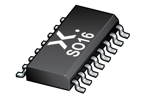
| NPIC6C596D | SO16 |
PCB Symbol, Footprint and 3D Model
| Model Name | 描述 |
|---|---|
|
|
封装
下表中的所有产品型号均已停产 。
| 型号 | 可订购的器件编号,(订购码(12NC)) | 状态 | 标示 | 封装 | 外形图 | 回流焊/波峰焊 | 包装 |
|---|---|---|---|---|---|---|---|
| NPIC6C596D | NPIC6C596D,118 (935297273118) |
Withdrawn / End-of-life |

SO16 (SOT109-1) |
SOT109-1 |
SO-SOJ-REFLOW
SO-SOJ-WAVE WAVE_BG-BD-1 |
SOT109-1_118 |
文档 (13)
| 文件名称 | 标题 | 类型 | 日期 |
|---|---|---|---|
| NPIC6C596 | Power logic 8-bit shift register; open-drain outputs | Data sheet | 2020-06-22 |
| AN11537 | Pin FMEA for NPIC Family | Application note | 2019-10-07 |
| AN90063 | Questions about package outline drawings | Application note | 2025-03-12 |
| SOT109-1 | 3D model for products with SOT109-1 package | Design support | 2020-01-22 |
| npic6c596 | NPIC6C596 IBIS model | IBIS model | 2016-05-30 |
| Nexperia_document_leaflet_Logic_NPIC_ShiftRegisters_201906 | NPIC Logic Shift Registers | Leaflet | 2019-07-12 |
| Nexperia_package_poster | Nexperia package poster | Leaflet | 2020-05-15 |
| SO16_SOT109-1_mk | plastic, small outline package; 16 leads; 1.27 mm pitch; 9.9 mm x 3.9 mm x 1.35 mm body | Marcom graphics | 2017-01-28 |
| SOT109-1 | plastic, small outline package; 16 leads; 1.27 mm pitch; 9.9 mm x 3.9 mm x 1.75 mm body | Package information | 2023-11-07 |
| NPIC6C596D_Nexperia_Product_Reliability | NPIC6C596D Nexperia Product Reliability | Quality document | 2022-05-04 |
| SO-SOJ-REFLOW | Footprint for reflow soldering | Reflow soldering | 2009-10-08 |
| SO-SOJ-WAVE | Footprint for wave soldering | Wave soldering | 2009-10-08 |
| WAVE_BG-BD-1 | Wave soldering profile | Wave soldering | 2021-09-08 |
Longevity
The Nexperia Longevity Program is aimed to provide our customers information from time to time about the expected time that our products can be ordered. The NLP is reviewed and updated regularly by our Executive Management Team. View our longevity program here.
PCB Symbol, Footprint and 3D Model
| Model Name | 描述 |
|---|---|
|
|
How does it work?
The interactive datasheets are based on the Nexperia MOSFET precision electrothermal models. With our interactive datasheets you can simply specify your own conditions interactively. Start by changing the values of the conditions. You can do this by using the sliders in the condition fields. By dragging the sliders you will see how the MOSFET will perform at the new conditions set.