
参数类型
| 型号 | VCC(A) (V) | VCC(B) (V) | Logic switching levels | Output drive capability (mA) | tpd (ns) | Nr of bits | Power dissipation considerations | Tamb (°C) | Rth(j-a) (K/W) | Ψth(j-top) (K/W) | Rth(j-c) (K/W) | Package name | Category |
|---|---|---|---|---|---|---|---|---|---|---|---|---|---|
| 74AXP1T45GW | 0.9 - 5.5 | 0.9 - 5.5 | CMOS | ± 12 | 9 | 1 | ultra low | -40~125 | 259 | 33.9 | 149 | TSSOP6 | Bi-directional | Direction controlled |
| 74AXP1T45GX | 0.9 - 5.5 | 0.9 - 5.5 | CMOS | ± 12 | 9 | 1 | ultra low | -40~125 | 460 | 13 | 229 | X2SON6 | Bi-directional | Direction controlled |
封装
| 型号 | 可订购的器件编号,(订购码(12NC)) | 状态 | 标示 | 封装 | 外形图 | 回流焊/波峰焊 | 包装 |
|---|---|---|---|---|---|---|---|
| 74AXP1T45GW | 74AXP1T45GWH (935690966125) |
Active | R5 |
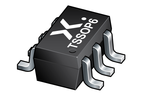
TSSOP6 (SOT363-2) |
SOT363-2 | SOT363-2_125 | |
| 74AXP1T45GX | 74AXP1T45GXZ (935690967147) |
Active | R5 |
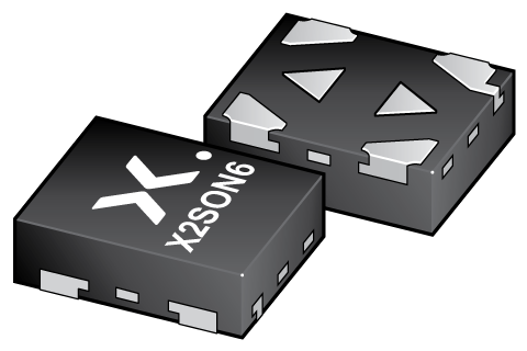
X2SON6 (SOT1255-2) |
SOT1255-2 | SOT1255-2_147 |
环境信息
| 型号 | 可订购的器件编号 | 化学成分 | RoHS | RHF指示符 |
|---|---|---|---|---|
| 74AXP1T45GW | 74AXP1T45GWH | 74AXP1T45GW |
|
|
| 74AXP1T45GX | 74AXP1T45GXZ | 74AXP1T45GX |
|
|
文档 (6)
| 文件名称 | 标题 | 类型 | 日期 |
|---|---|---|---|
| 74AXP1T45 | 1-bit dual supply translating transceiver; 3-state | Data sheet | 2024-07-25 |
| AN90029 | Pin FMEA for AXPnT family | Application note | 2021-07-13 |
| SOT363-2 | 3D model for products with SOT363-2 package | Design support | 2023-02-02 |
| SOT1255-2 | 3D model for products with SOT1255-2 package | Design support | 2021-01-28 |
| SOT363-2 | plastic thin shrink small outline package; 6 leads; body width 1.25 mm | Package information | 2022-11-21 |
| SOT1255-2 | plastic thermal enhanced extremely thin small outline package; no leads;6 terminals; body 1.0 x 0.8 x 0.32 mm | Package information | 2020-08-27 |
支持
如果您需要设计/技术支持,请告知我们并填写 应答表 我们会尽快回复您。
Ordering, pricing & availability
样品
作为 Nexperia 的客户,您可以通过我们的销售机构订购样品。
如果您没有 Nexperia 的直接账户,我们的全球和地区分销商网络可为您提供 Nexperia 样品支持。查看官方经销商列表。