74LVC16240A
16-bit buffer/line driver with 5V tolerant inputs/outputs; inverting; 3-state
The 74LVC16240A is a 16-bit inverting buffer/line driver with 3-state outputs. The device can be used as four 4-bit buffers, two 8-bit buffers or one 16-bit buffer. The device features four output enables (1OE, 2OE, 3OE and 4OE), each controlling four of the 3-state outputs. A HIGH on nOE causes the outputs to assume a high-impedance OFF-state.
Inputs can be driven from either 3.3 V or 5 V devices. When disabled, up to 5.5 V can be applied to the outputs. These features allow the use of these devices in mixed 3.3 V and 5 V applications.
This device is fully specified for partial power-down applications using IOFF. The IOFF circuitry disables the output, preventing the damaging backflow current through the device when it is powered down.
Features and benefits
5 V tolerant inputs/outputs for interfacing with 5 V logic
Wide supply voltage range from 1.2 V to 3.6 V
CMOS low power consumption
MULTIBYTE flow-through standard pin-out architecture
Low inductance multiple power and ground pins for minimum noise and ground bounce
Direct interface with TTL levels
Complies with JEDEC standard:
JESD8-7A (1.65 V to 1.95 V)
JESD8-5A (2.3 V to 2.7 V)
JESD8-C/JESD36 (2.7 V to 3.6 V)
ESD protection:
HBM: ANSI/ESDA/JEDEC JS-001 class 2 exceeds 2000 V
CDM: ANSI/ESDA/JEDEC JS-002 class C3 exceeds 1000 V
Specified from -40 °C to +85 °C and from -40 °C to +125 °C.
参数类型
| 型号 | VCC (V) | Logic switching levels | Output drive capability (mA) | fmax (MHz) | Nr of bits | Power dissipation considerations | Tamb (°C) | Package name |
|---|---|---|---|---|---|---|---|---|
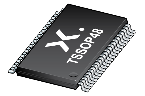
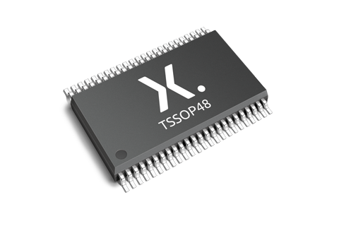
| 74LVC16240ADGG | 1.2 - 3.6 | CMOS/LVTTL | ± 24 | 175 | 16 | low | -40~125 | TSSOP48 |
封装
| 型号 | 可订购的器件编号,(订购码(12NC)) | 状态 | 标示 | 封装 | 外形图 | 回流焊/波峰焊 | 包装 |
|---|---|---|---|---|---|---|---|
| 74LVC16240ADGG | 74LVC16240ADGG,118 (935235110118) |
Active | LVC16240A |
TSSOP48 (SOT362-1) |
SOT362-1 |
SSOP-TSSOP-VSO-WAVE
|
SOT362-1_118 |
文档 (11)
| 文件名称 | 标题 | 类型 | 日期 |
|---|---|---|---|
| 74LVC16240A | 16-bit buffer/line driver with 5V tolerant inputs/outputs; inverting; 3-state | Data sheet | 2024-03-20 |
| AN11009 | Pin FMEA for LVC family | Application note | 2019-01-09 |
| AN263 | Power considerations when using CMOS and BiCMOS logic devices | Application note | 2023-02-07 |
| 001aaa439 | Block diagram: 74LVC16240ADGG, 74LVC16240ADL | Block diagram | 2009-11-04 |
| SOT362-1 | 3D model for products with SOT362-1 package | Design support | 2020-01-22 |
| lvc16240a | lvc16240a IBIS model | IBIS model | 2013-04-08 |
| Nexperia_package_poster | Nexperia package poster | Leaflet | 2020-05-15 |
| TSSOP48_SOT362-1_mk | plastic, thin shrink small outline package; 48 leads; 0.5 mm pitch; 12.8 mm x 6.1 mm x 1.2 mm body | Marcom graphics | 2017-01-28 |
| SOT362-1 | plastic thin shrink small outline package; 48 leads; body width 6.1 mm | Package information | 2024-01-05 |
| Nexperia_Selection_guide_2023 | Nexperia Selection Guide 2023 | Selection guide | 2023-05-10 |
| SSOP-TSSOP-VSO-WAVE | Footprint for wave soldering | Wave soldering | 2009-10-08 |
支持
如果您需要设计/技术支持,请告知我们并填写 应答表 我们会尽快回复您。
Ordering, pricing & availability
样品
作为 Nexperia 的客户,您可以通过我们的销售机构订购样品。
如果您没有 Nexperia 的直接账户,我们的全球和地区分销商网络可为您提供 Nexperia 样品支持。查看官方经销商列表。