参数类型
| 型号 |
|---|
封装
下表中的所有产品型号均已停产 。
| 型号 | 可订购的器件编号,(订购码(12NC)) | 状态 | 标示 | 封装 | 外形图 | 回流焊/波峰焊 | 包装 |
|---|---|---|---|---|---|---|---|
| 74LVT16500ADGG | 74LVT16500ADGG,112 (935203020112) |
Obsolete | LVT16500A Standard Procedure Standard Procedure |
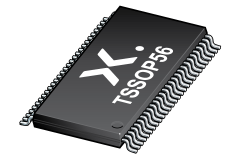
TSSOP56 (SOT364-1) |
SOT364-1 |
SSOP-TSSOP-VSO-WAVE
|
暂无信息 |
| 74LVT16500ADGG,118 (935203020118) |
Obsolete | LVT16500A Standard Procedure Standard Procedure | SOT364-1_118 | ||||
| 74LVT16500ADGGS (935203020512) |
Obsolete | LVT16500A Standard Procedure Standard Procedure | 暂无信息 | ||||
| 74LVT16500ADGGY (935203020518) |
Obsolete | LVT16500A Standard Procedure Standard Procedure | 暂无信息 |
环境信息
下表中的所有产品型号均已停产 。
| 型号 | 可订购的器件编号 | 化学成分 | RoHS | RHF指示符 |
|---|---|---|---|---|
| 74LVT16500ADGG | 74LVT16500ADGG,112 | 74LVT16500ADGG |
|
|
| 74LVT16500ADGG | 74LVT16500ADGG,118 | 74LVT16500ADGG |
|
|
| 74LVT16500ADGG | 74LVT16500ADGGS | 74LVT16500ADGG |
|
|
| 74LVT16500ADGG | 74LVT16500ADGGY | 74LVT16500ADGG |
|
|
文档 (12)
| 文件名称 | 标题 | 类型 | 日期 |
|---|---|---|---|
| 74LVT16500A | 3.3 V 18-bit universal bus transceiver; 3-state | Data sheet | 2006-05-28 |
| 001aaf035 | Block diagram: 74LVT16500ADGG, 74LVT16500ADL | Block diagram | 2009-11-04 |
| 001aaf038 | Block diagram: 74LVT16500ADGG, 74LVT16500ADL | Block diagram | 2009-11-04 |
| 001aaf039 | Block diagram: 74LVT16500ADGG, 74LVT16500ADL | Block diagram | 2009-11-04 |
| 001aaf040 | Block diagram: 74LVT16500ADGG, 74LVT16500ADL | Block diagram | 2009-11-04 |
| SOT364-1 | 3D model for products with SOT364-1 package | Design support | 2020-01-22 |
| lvt16500a | lvt16500a IBIS model | IBIS model | 2013-04-09 |
| Nexperia_package_poster | Nexperia package poster | Leaflet | 2020-05-15 |
| SOT364-1 | plastic, thin shrink small outline package; 56 leads; 0.5 mm pitch; 14 mm x 6.1 mm x 1.2 mm body | Package information | 2022-06-23 |
| lvt16 | lvt16 Spice model | SPICE model | 2013-05-07 |
| Nexperia_Selection_guide_2023 | Nexperia Selection Guide 2023 | Selection guide | 2023-05-10 |
| SSOP-TSSOP-VSO-WAVE | Footprint for wave soldering | Wave soldering | 2009-10-08 |
支持
如果您需要设计/技术支持,请告知我们并填写 应答表 我们会尽快回复您。
Ordering, pricing & availability
样品
作为 Nexperia 的客户,您可以通过我们的销售机构订购样品。
如果您没有 Nexperia 的直接账户,我们的全球和地区分销商网络可为您提供 Nexperia 样品支持。查看官方经销商列表。