Register once, drag and drop ECAD models into your CAD tool and speed up your design.
Click here for more informationPBSS4021SN
20 V, 7.5 A NPN/NPN low V_CEsat (BISS) transistor
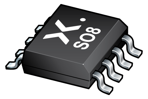
NPN/NPN low VCEsat Breakthrough In Small Signal (BISS) transistor in a SOT96-1 (SO8) medium power Surface-Mounted Device (SMD) plastic package.
NPN/PNP complement: PBSS4021SPN
Features and benefits
- Very low collector-emitter saturation voltage VCEsat
- High collector current capability IC and ICM
- High collector current gain (hFE) at high IC
- High efficiency due to less heat generation
- Smaller required Printed-Circuit Board (PCB) area than for conventional transistors
Applications
- Loadswitch
- Battery-driven devices
- Power management
- Charging circuits
- Power switches (e.g. motors, fans)
参数类型
| 型号 | Package version | Package name | Size (mm) | channel type (e) | Configuration | Ptot (mW) | VCEO [max] (V) | IC [max] (mA) | hFE [min] | Automotive qualified |
|---|---|---|---|---|---|---|---|---|---|---|
| PBSS4021SN | SOT96-1 | SO8 | 4.9 x 3.9 x 1.75 | NPN | 2 | 730.0 | 20.0 | 7500.0 | 300.0 | N |
封装
下表中的所有产品型号均已停产 。
| 型号 | 可订购的器件编号,(订购码(12NC)) | 状态 | 标示 | 封装 | 外形图 | 回流焊/波峰焊 | 包装 |
|---|---|---|---|---|---|---|---|
| PBSS4021SN | PBSS4021SN,115 (934063408115) |
Withdrawn / End-of-life | 4021SN |

SO8 (SOT96-1) |
SOT96-1 |
SO-SOJ-REFLOW
SO-SOJ-WAVE WAVE_BG-BD-1 |
SOT96-1_115 |
文档 (12)
| 文件名称 | 标题 | 类型 | 日期 |
|---|---|---|---|
| PBSS4021SN | 20 V, 7.5 A NPN/NPN low V_CEsat (BISS) transistor | Data sheet | 2018-08-28 |
| AN10909 | Low VCEsat transistors in medium power loadswitch applications | Application note | 2013-03-14 |
| AN11045 | Next generation of NXP low VCEsat transistors: improved technology for discrete semiconductors | Application note | 2013-03-04 |
| AN11076 | Thermal behavior of small-signal discretes on multilayer PCBs | Application note | 2021-06-23 |
| Nexperia_package_poster | Nexperia package poster | Leaflet | 2020-05-15 |
| SO8_SOT96-1_mk | plastic, small outline package; 8 leads; 1.27 mm pitch; 4.9 mm x 3.9 mm x 1.75 mm body | Marcom graphics | 2017-01-28 |
| SOT96-1 | plastic, small outline package; 8 leads; 1.27 mm pitch; 4.9 mm x 3.9 mm x 1.75 mm body | Package information | 2020-04-21 |
| PBSS4021SN_Nexperia_Product_Reliability | PBSS4021SN Nexperia Product Reliability | Quality document | 2019-04-29 |
| SO-SOJ-REFLOW | Footprint for reflow soldering | Reflow soldering | 2009-10-08 |
| PBSS4021SN | PBSS4021SN SPICE model | SPICE model | 2024-08-27 |
| SO-SOJ-WAVE | Footprint for wave soldering | Wave soldering | 2009-10-08 |
| WAVE_BG-BD-1 | Wave soldering profile | Wave soldering | 2021-09-08 |
Longevity
The Nexperia Longevity Program is aimed to provide our customers information from time to time about the expected time that our products can be ordered. The NLP is reviewed and updated regularly by our Executive Management Team. View our longevity program here.
模型
| 文件名称 | 标题 | 类型 | 日期 |
|---|---|---|---|
| PBSS4021SN | PBSS4021SN SPICE model | SPICE model | 2024-08-27 |
How does it work?
The interactive datasheets are based on the Nexperia MOSFET precision electrothermal models. With our interactive datasheets you can simply specify your own conditions interactively. Start by changing the values of the conditions. You can do this by using the sliders in the condition fields. By dragging the sliders you will see how the MOSFET will perform at the new conditions set.