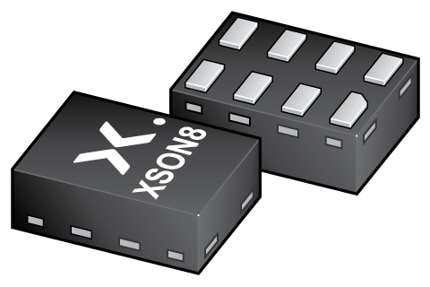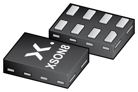
Register once, drag and drop ECAD models into your CAD tool and speed up your design.
Click here for more information74LVC2G53GF
2-channel analog multiplexer/demultiplexer
The 74LVC2G53 is a single-pole double-throw analog switch with a digital select input (S), two independent inputs/outputs (Y0 and Y1), a common input/output (Z) and a digital enable input (E). When E is HIGH, the switch is turned off. Inputs can be driven from either 3.3 V or 5 V devices. This feature allows the use of these devices as translators in mixed 3.3 V and 5 V environments.
Schmitt trigger action at the select and enable inputs makes the circuit tolerant of slower input rise and fall times across the entire VCC range from 1.65 V to 5.5 V.
Alternatives
Features and benefits
Wide supply voltage range from 1.65 V to 5.5 V
Very low ON resistance:
7.5 Ω (typical) at VCC = 2.7 V
6.5 Ω (typical) at VCC = 3.3 V
6 Ω (typical) at VCC = 5 V
Switch current capability of 32 mA
High noise immunity
CMOS low-power consumption
Overvoltage tolerant inputs to 5.5 V
TTL interface compatibility at 3.3 V
Latch-up performance meets requirements of JESD 78 Class I
ESD protection:
HBM: ANSI/ESDA/JEDEC JS-001 class 2 exceeds 2000 V
CDM: ANSI/ESDA/JEDEC JS-002 class C3 exceeds 1000 V
Multiple package options
Specified from -40 °C to +85 °C and from -40 °C to +125 °C
参数类型
| 型号 | Package name |
|---|---|
| 74LVC2G53GF | XSON8 |
PCB Symbol, Footprint and 3D Model
| Model Name | 描述 |
|---|---|
|
|
封装
下表中的所有产品型号均已停产 。
| 型号 | 可订购的器件编号,(订购码(12NC)) | 状态 | 标示 | 封装 | 外形图 | 回流焊/波峰焊 | 包装 |
|---|---|---|---|---|---|---|---|
| 74LVC2G53GF | 74LVC2G53GF,115 (935291509115) |
Obsolete | V3 |

XSON8 (SOT1089) |
SOT1089 |
REFLOW_BG-BD-1
|
SOT1089_115 |
文档 (11)
| 文件名称 | 标题 | 类型 | 日期 |
|---|---|---|---|
| 74LVC2G53 | 2-channel analog multiplexer/demultiplexer | Data sheet | 2023-08-28 |
| AN11009 | Pin FMEA for LVC family | Application note | 2019-01-09 |
| AN90063 | Questions about package outline drawings | Application note | 2025-03-12 |
| Nexperia_document_guide_MiniLogic_MicroPak_201808 | MicroPak leadless logic portfolio guide | Brochure | 2018-09-03 |
| SOT1089 | 3D model for products with SOT1089 package | Design support | 2019-10-07 |
| lvc2g53 | 74LVC2G53 IBIS model | IBIS model | 2015-02-19 |
| Nexperia_package_poster | Nexperia package poster | Leaflet | 2020-05-15 |
| XSON8_SOT1089_mk | plastic, extremely thin small outline package; no leads; 8 terminals; 0.55 mm pitch; 1.35 mm x 1 mm x 0.5 mm body | Marcom graphics | 2017-01-28 |
| SOT1089 | plastic, leadless extremely thin small outline package; 8 terminals; 0.35 mm pitch; 1.35 mm x 1 mm x 0.5 mm body | Package information | 2022-06-03 |
| REFLOW_BG-BD-1 | Reflow soldering profile | Reflow soldering | 2021-04-06 |
| MAR_SOT1089 | MAR_SOT1089 Topmark | Top marking | 2013-06-03 |
Longevity
The Nexperia Longevity Program is aimed to provide our customers information from time to time about the expected time that our products can be ordered. The NLP is reviewed and updated regularly by our Executive Management Team. View our longevity program here.
PCB Symbol, Footprint and 3D Model
| Model Name | 描述 |
|---|---|
|
|
How does it work?
The interactive datasheets are based on the Nexperia MOSFET precision electrothermal models. With our interactive datasheets you can simply specify your own conditions interactively. Start by changing the values of the conditions. You can do this by using the sliders in the condition fields. By dragging the sliders you will see how the MOSFET will perform at the new conditions set.
