Register once, drag and drop ECAD models into your CAD tool and speed up your design.
Click here for more informationCBT3253ADB
Dual 1-of-4 FET multiplexer/demultiplexer
The CBT3253A is a dual single-pole,4-throw bus switch. The device features two output enable inputs ( nOE) and two select inputs (S0 and S1). When nOE are LOW the switch is enabled and the select inputs can be used to connect the nA terminal to one of the four associated nB terminals.
Alternatives
Features and benefits
5 Ω switch connection between two ports
Direct interface with TTL levels
Overvoltage tolerant control inputs to 5.5 V
Minimal propagation delay through the switch
Latch-up protection exceeds 100 mA per JEDEC standard JESD78 class II level A
ESD protection:
HBM: ANSI/ESDA/JEDEC JS-001 class 2 exceeds 2000 V
CDM: ANSI/ESDA/JEDEC JS-002 class C3 exceeds 1000 V
Multiple package options
Specified from -40 °C to +85 °C
参数类型
| 型号 | Package name |
|---|---|
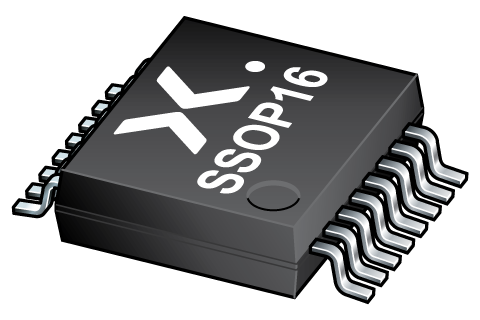
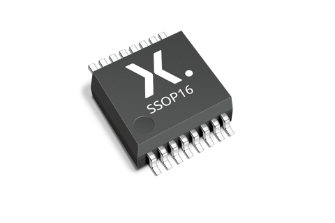
| CBT3253ADB | SSOP16 |
PCB Symbol, Footprint and 3D Model
| Model Name | 描述 |
|---|---|
|
|
封装
下表中的所有产品型号均已停产 。
| 型号 | 可订购的器件编号,(订购码(12NC)) | 状态 | 标示 | 封装 | 外形图 | 回流焊/波峰焊 | 包装 |
|---|---|---|---|---|---|---|---|
| CBT3253ADB | CBT3253ADB,112 (935275885112) |
Obsolete | C3253A |
SSOP16 (SOT338-1) |
SOT338-1 |
SSOP-TSSOP-VSO-REFLOW
SSOP-TSSOP-VSO-WAVE |
暂无信息 |
| CBT3253ADB,118 (935275885118) |
Obsolete | C3253A | 暂无信息 |
环境信息
下表中的所有产品型号均已停产 。
| 型号 | 可订购的器件编号 | 化学成分 | RoHS | RHF指示符 |
|---|---|---|---|---|
| CBT3253ADB | CBT3253ADB,112 | CBT3253ADB |
|
|
| CBT3253ADB | CBT3253ADB,118 | CBT3253ADB |
|
|
文档 (7)
| 文件名称 | 标题 | 类型 | 日期 |
|---|---|---|---|
| AN90010 | Pin FMEA for CBT(D) family | Application note | 2019-10-28 |
| cbt3253a | cbt3253a IBIS model | IBIS model | 2017-06-02 |
| Nexperia_package_poster | Nexperia package poster | Leaflet | 2020-05-15 |
| SSOP16_SOT338-1_mk | plastic, shrink small outline package; 16 leads; 0.65 mm pitch; 6.2 mm x 5.3 mm x 2 mm body | Marcom graphics | 2017-01-28 |
| SOT338-1 | plastic, shrink small outline package; 16 leads; 0.65 mm pitch; 6.2 mm x 5.3 mm x 2 mm body | Package information | 2022-06-20 |
| SSOP-TSSOP-VSO-REFLOW | Footprint for reflow soldering | Reflow soldering | 2009-10-08 |
| SSOP-TSSOP-VSO-WAVE | Footprint for wave soldering | Wave soldering | 2009-10-08 |
Longevity
The Nexperia Longevity Program is aimed to provide our customers information from time to time about the expected time that our products can be ordered. The NLP is reviewed and updated regularly by our Executive Management Team. View our longevity program here.
模型
| 文件名称 | 标题 | 类型 | 日期 |
|---|---|---|---|
| cbt3253a | cbt3253a IBIS model | IBIS model | 2017-06-02 |
PCB Symbol, Footprint and 3D Model
| Model Name | 描述 |
|---|---|
|
|
How does it work?
The interactive datasheets are based on the Nexperia MOSFET precision electrothermal models. With our interactive datasheets you can simply specify your own conditions interactively. Start by changing the values of the conditions. You can do this by using the sliders in the condition fields. By dragging the sliders you will see how the MOSFET will perform at the new conditions set.
CBT3253ADB
Dual 1-of-4 FET multiplexer/demultiplexer
从安世半导体购买
| SKU | 库存* | MOQ | 单位价格 | 数量 |
|---|