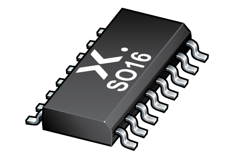
可订购部件
| 型号 | 可订购的器件编号 | 订购代码(12NC) | 封装 | 从经销商处购买 |
|---|---|---|---|---|
| 74LVC163D | 74LVC163D,118 | 935210540118 | SOT109-1 | 订单产品 |

Register once, drag and drop ECAD models into your CAD tool and speed up your design.
Click here for more informationPresettable synchronous 4-bit binary counter; synchronous reset
The 74LVC163 is a synchronous presettable binary counter which features an internal look-ahead carry and can be used for high-speed counting. Synchronous operation is provided by having all flip-flops clocked simultaneously on the positive-going edge of the clock (pin CP). The outputs (pins Q0 to Q3) of the counters may be preset to a HIGH-level or LOW-level. A LOW-level at the parallel enable input (pin PE) disables the counting action and causes the data at the data inputs (pins D0 to D3) to be loaded into the counter on the positive-going edge of the clock (provided that the set-up and hold time requirements for PE are met). Preset takes place regardless of the levels at count enable inputs (pin CEP and CET). A LOW-level at the master reset input (pin MR) sets all four outputs of the flip-flops (pins Q0 to Q3) to LOW-level after the next positive-going transition on the clock input (pin CP) (provided that the set-up and hold time requirements for PE are met). This action occurs regardless of the levels at input pins PE, CET and CEP. This synchronous reset feature enables the designer to modify the maximum count with only one external NAND gate.
The look-ahead carry simplifies serial cascading of the counters. Both count enable inputs (pin CEP and CET) must be HIGH in count. The CET input is fed forward to enable the terminal count output (pin TC). The TC output thus enabled will produce a HIGH output pulse of a duration approximately equal to a HIGH-level output of Q0. This pulse can be used to enable the next cascaded stage.
The maximum clock frequency for the cascaded counters is determined by tPHL (propagation delay CP to TC) and tsu (set-up time CEP to CP) according to the formula: .
Wide supply voltage range from 1.2 V to 3.6 V
Inputs accept voltages up to 5.5 V
CMOS low power consumption
Direct interface with TTL levels
Synchronous reset
Synchronous counting and loading
Two count enable inputs for n-bit cascading
Positive edge-triggered clock
Complies with JEDEC standard:
JESD8-7A (1.65 V to 1.95 V)
JESD8-5A (2.3 V to 2.7 V)
JESD8-C/JESD36 (2.7 V to 3.6 V)
ESD protection:
HBM: ANSI/ESDA/JEDEC JS-001 class 2 exceeds 2000 V
CDM: ANSI/ESDA/JEDEC JS-002 class C3 exceeds 1000 V
Specified from -40 °C to +85 °C and -40 °C to 125 °C
| 型号 | VCC (V) | Output drive capability (mA) | Logic switching levels | tpd (ns) | Power dissipation considerations | Tamb (°C) | Rth(j-a) (K/W) | Ψth(j-top) (K/W) | Rth(j-c) (K/W) | Package name |
|---|---|---|---|---|---|---|---|---|---|---|
| 74LVC163D | 1.2 - 3.6 | ± 24 | CMOS/LVTTL | 4.9 | low | -40~125 | 92 | 9.6 | 51.7 | SO16 |
| Model Name | 描述 |
|---|---|
|
|
| 型号 | 可订购的器件编号,(订购码(12NC)) | 状态 | 标示 | 封装 | 外形图 | 回流焊/波峰焊 | 包装 |
|---|---|---|---|---|---|---|---|
| 74LVC163D | 74LVC163D,118 (935210540118) |
Active | 74LVC163D |

SO16 (SOT109-1) |
SOT109-1 |
SO-SOJ-REFLOW
SO-SOJ-WAVE WAVE_BG-BD-1 |
SOT109-1_118 |
| 文件名称 | 标题 | 类型 | 日期 |
|---|---|---|---|
| 74LVC163 | Presettable synchronous 4-bit binary counter; synchronous reset | Data sheet | 2024-02-12 |
| AN11009 | Pin FMEA for LVC family | Application note | 2019-01-09 |
| AN263 | Power considerations when using CMOS and BiCMOS logic devices | Application note | 2023-02-07 |
| AN90063 | Questions about package outline drawings | Application note | 2025-03-12 |
| SOT109-1 | 3D model for products with SOT109-1 package | Design support | 2020-01-22 |
| lvc163 | lvc163 IBIS model | IBIS model | 2013-04-08 |
| Nexperia_package_poster | Nexperia package poster | Leaflet | 2020-05-15 |
| SO16_SOT109-1_mk | plastic, small outline package; 16 leads; 1.27 mm pitch; 9.9 mm x 3.9 mm x 1.35 mm body | Marcom graphics | 2017-01-28 |
| SOT109-1 | plastic, small outline package; 16 leads; 1.27 mm pitch; 9.9 mm x 3.9 mm x 1.75 mm body | Package information | 2023-11-07 |
| SOT109-1_118 | SO16; Reel pack for SMD, 13"; Q1/T1 product orientation | Packing information | 2024-02-19 |
| 74LVC163D_Nexperia_Product_Reliability | 74LVC163D Nexperia Product Reliability | Quality document | 2025-03-20 |
| SO-SOJ-REFLOW | Footprint for reflow soldering | Reflow soldering | 2009-10-08 |
| lvc | lvc Spice model | SPICE model | 2013-05-07 |
| SO-SOJ-WAVE | Footprint for wave soldering | Wave soldering | 2009-10-08 |
| WAVE_BG-BD-1 | Wave soldering profile | Wave soldering | 2021-09-08 |
The Nexperia Longevity Program is aimed to provide our customers information from time to time about the expected time that our products can be ordered. The NLP is reviewed and updated regularly by our Executive Management Team. View our longevity program here.
| Model Name | 描述 |
|---|---|
|
|
| 型号 | Orderable part number | Ordering code (12NC) | 状态 | 包装 | Packing Quantity | 在线购买 |
|---|---|---|---|---|---|---|
| 74LVC163D | 74LVC163D,118 | 935210540118 | Active | SOT109-1_118 | 2,500 |
|
作为 Nexperia 的客户,您可以通过我们的销售机构订购样品。
如果您没有 Nexperia 的直接账户,我们的全球和地区分销商网络可为您提供 Nexperia 样品支持。查看官方经销商列表。
The interactive datasheets are based on the Nexperia MOSFET precision electrothermal models. With our interactive datasheets you can simply specify your own conditions interactively. Start by changing the values of the conditions. You can do this by using the sliders in the condition fields. By dragging the sliders you will see how the MOSFET will perform at the new conditions set.