可订购部件
| 型号 | 可订购的器件编号 | 订购代码(12NC) | 封装 | 从经销商处购买 |
|---|---|---|---|---|
| 74ALVCH16821DGG | 74ALVCH16821DGG,11 | 935259010118 | SOT364-1 | 订单产品 |
Register once, drag and drop ECAD models into your CAD tool and speed up your design.
Click here for more information20-bit bus-interface D-type flip-flop; positive-edge trigger; 3-state
The 74ALVCH16821 has two 10-bit, edge triggered registers, with each register coupled to a 3-state output buffer. The two sections of each register are controlled independently by the clock (nCP) and output enable nOE control gates.
Each register is fully edge triggered. The state of each nDn input, one set-up time before the LOW-to-HIGH clock transition, is transferred to the corresponding flip-flop’s nQn output.
When nOE is LOW, the data in the register appears at the outputs. When nOE is HIGH, the outputs are in high impedance OFF state. Operation of the nOE input does not affect the state of the flip-flops.
The 74ALVCH16821 has active bus hold circuitry which is provided to hold unused or floating data inputs at a valid logic level. This feature eliminates the need for external pull-up or pull-down resistors.
Wide supply voltage range from 1.2 V to 3.6 V
CMOS low-power consumption
Direct interface with TTL levels
Current drive ± 24 mA at 3.0 V
MULTIBYTE™ flow-through standard pin-out architecture
Low inductance multiple VCC and GND pins for minimum noise and ground bounce
Output drive capability 50 Ω transmission lines at 85°C
All data inputs have bushold
Complies with JEDEC standard no. 8-1A
Complies with JEDEC standards:
JESD8-5 (2.3 V to 2.7 V)
JESD8B/JESD36 (2.7 V to 3.6 V)
ESD protection:
| 型号 | VCC (V) | Logic switching levels | Output drive capability (mA) | tpd (ns) | fmax (MHz) | Power dissipation considerations | Tamb (°C) | Package name |
|---|---|---|---|---|---|---|---|---|
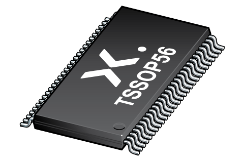
| 74ALVCH16821DGG | 1.2 - 3.6 | TTL | ± 24 | 2.5 | 350 | low | -40~85 | TSSOP56 |
| 型号 | 可订购的器件编号,(订购码(12NC)) | 状态 | 标示 | 封装 | 外形图 | 回流焊/波峰焊 | 包装 |
|---|---|---|---|---|---|---|---|
| 74ALVCH16821DGG | 74ALVCH16821DGG,11 (935259010118) |
Active | ALVCH16821 |
TSSOP56 (SOT364-1) |
SOT364-1 |
SSOP-TSSOP-VSO-WAVE
|
SOT364-1_118 |
| 文件名称 | 标题 | 类型 | 日期 |
|---|---|---|---|
| 74ALVCH16821 | 20-bit bus-interface D-type flip-flop; positive-edge trigger; 3-state | Data sheet | 2024-07-09 |
| SOT364-1 | 3D model for products with SOT364-1 package | Design support | 2020-01-22 |
| alvch16821 | alvch16821 IBIS model | IBIS model | 2013-04-08 |
| Nexperia_package_poster | Nexperia package poster | Leaflet | 2020-05-15 |
| SOT364-1 | plastic, thin shrink small outline package; 56 leads; 0.5 mm pitch; 14 mm x 6.1 mm x 1.2 mm body | Package information | 2022-06-23 |
| SOT364-1_118 | TSSOP56; Reel pack for SMD, 13"; Q1/T1 product orientation | Packing information | 2020-04-21 |
| 74ALVCH16821DGG_Nexperia_Product_Reliability | 74ALVCH16821DGG Nexperia Product Reliability | Quality document | 2024-06-16 |
| SSOP-TSSOP-VSO-WAVE | Footprint for wave soldering | Wave soldering | 2009-10-08 |
如果您需要设计/技术支持,请告知我们并填写 应答表 我们会尽快回复您。
| 文件名称 | 标题 | 类型 | 日期 |
|---|---|---|---|
| alvch16821 | alvch16821 IBIS model | IBIS model | 2013-04-08 |
| SOT364-1 | 3D model for products with SOT364-1 package | Design support | 2020-01-22 |
| 型号 | Orderable part number | Ordering code (12NC) | 状态 | 包装 | Packing Quantity | 在线购买 |
|---|---|---|---|---|---|---|
| 74ALVCH16821DGG | 74ALVCH16821DGG,11 | 935259010118 | Active | SOT364-1_118 | 2,000 | 订单产品 |
作为 Nexperia 的客户,您可以通过我们的销售机构订购样品。
如果您没有 Nexperia 的直接账户,我们的全球和地区分销商网络可为您提供 Nexperia 样品支持。查看官方经销商列表。
The interactive datasheets are based on the Nexperia MOSFET precision electrothermal models. With our interactive datasheets you can simply specify your own conditions interactively. Start by changing the values of the conditions. You can do this by using the sliders in the condition fields. By dragging the sliders you will see how the MOSFET will perform at the new conditions set.
20-bit bus-interface D-type flip-flop; positive-edge trigger; 3-state
| SKU | 库存* | MOQ | 单位价格 | 数量 |
|---|