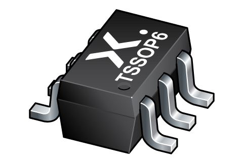
Input Polarity Protected, Low IQ Ideal Diode evaluation board (NID5100)
The NEVB-NID5100 evaluation board is a two-layer PCB equipped with two NID5100 ideal diodes. It allows users to explore the device's behavior under various application conditions like:
OR-ing two supplies, reverse polarity protection, reverse current blocking and ORing with an external Mosfet
Key features & benefits
• Input operating voltage range (VIN) 1.2V to 5.5V
• Continuous output current 1.5A
• Three supply inputs
• Two additional USB-C supply inputs
• Access to all device pins
• Use case selection by means of jumpers
文档 (1)
| 文件名称 | 标题 | 类型 | 日期 |
|---|---|---|---|
| UM90040 | NID5100, 1.2 V to 5.5 V, 1.5 A input polarity protected, low quiescent current ideal diode evaluation board | User manual | 2024-07-25 |
