
74LVC1G99
Ultra-configurable multiple function gate; 3-state
The 74LVC1G99 provides a low voltage, ultra-configurable, multiple function gate with 3-state output. The device can be configured as one of several logic functions including, AND, OR, NAND, NOR, XOR, XNOR, inverter, buffer and MUX. No external components are required to configure the device as all inputs can be connected directly to VCC or GND. The 3-state output is controlled by the output enable input (OE). A HIGH level at OE causes the output (Y) to assume a high-impedance OFF-state. When OE is LOW, the output state is determined by the signals applied to the Schmitt trigger inputs (A, B, C and D).
Due to the use of Schmitt trigger inputs the device is tolerant of slowly changing input signals, transforming them into sharply defined, jitter free output signals. By eliminating leakage current paths to VCC and GND, the inputs and disabled output are also over-voltage tolerant, making the device suitable for mixed-voltage applications.
This device is fully specified for partial power-down applications using IOFF. The IOFF circuitry disables the output, preventing the damaging backflow current through the device when it is powered down.
The 74LVC1G99 is fully specified over the supply range from 1.65 V to 5.5 V.
Features and benefits
Wide supply voltage range from 1.65 V to 5.5 V
5 V tolerant inputs for interfacing with 5 V logic
High noise immunity
±24 mA output drive (VCC = 3.0 V)
CMOS low power consumption
Latch-up performance exceeds 250 mA
Direct interface with TTL levels
Inputs accept voltages up to 5 V
Complies with JEDEC standard:
JESD8-7 (1.65 V to 1.95 V)
JESD8-5 (2.3 V to 2.7 V)
JESD8-B/JESD36 (2.7 V to 3.6 V)
ESD protection:
HBM: ANSI/ESDA/JEDEC JS-001 class 2 exceeds 2000 V
CDM: ANSI/ESDA/JEDEC JS-002 class C3 exceeds 1000 V
Multiple package options
Specified from -40 °C to +85 °C and -40 °C to +125 °C.
参数类型
| 型号 | VCC (V) | Logic switching levels | Output drive capability (mA) | tpd (ns) | fmax (MHz) | Nr of bits | Power dissipation considerations | Tamb (°C) | Package name |
|---|---|---|---|---|---|---|---|---|---|
| 74LVC1G99DP | 1.65 - 5.5 | TTL | ± 32 | 8.4 | 150 | 1 | low | -40~125 | TSSOP8 |
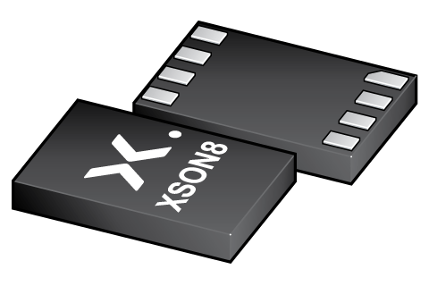
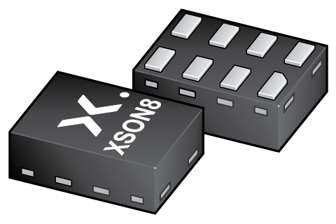
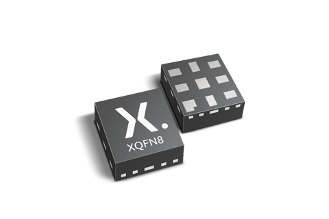
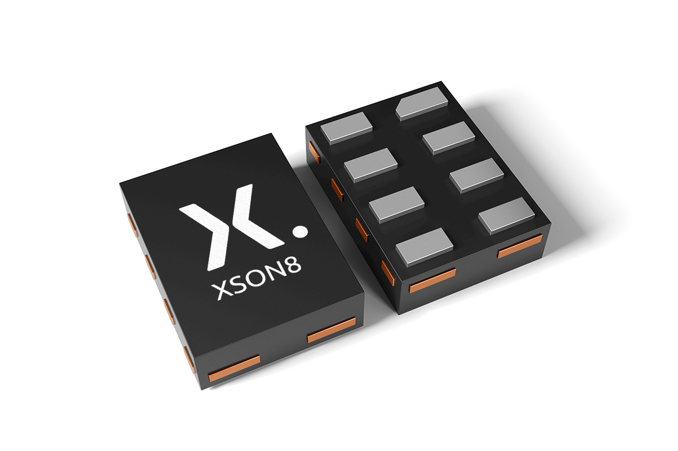
| 74LVC1G99GN | 1.65 - 5.5 | TTL | ± 32 | 8.4 | 150 | 1 | low | -40~125 | XSON8 |
| 74LVC1G99GS | 1.65 - 5.5 | TTL | ± 32 | 8.4 | 150 | 1 | low | -40~125 | XSON8 |
| 74LVC1G99GT | 1.65 - 5.5 | TTL | ± 32 | 8.4 | 150 | 1 | low | -40~125 | XSON8 |
封装
| 型号 | 可订购的器件编号,(订购码(12NC)) | 状态 | 标示 | 封装 | 外形图 | 回流焊/波峰焊 | 包装 |
|---|---|---|---|---|---|---|---|
| 74LVC1G99DP | 74LVC1G99DP,125 (935284435125) |
Active | V99 |
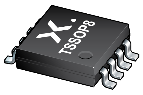
TSSOP8 (SOT505-2) |
SOT505-2 | SOT505-2_125 | |
| 74LVC1G99GN | 74LVC1G99GN,115 (935288987115) |
Active | YF |
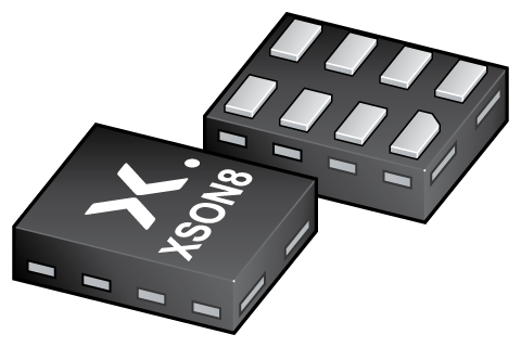
XSON8 (SOT1116) |
SOT1116 |
REFLOW_BG-BD-1
|
SOT1116_115 |
| 74LVC1G99GS | 74LVC1G99GS,115 (935292796115) |
Active | YF |
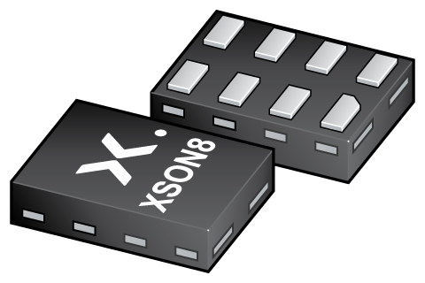
XSON8 (SOT1203) |
SOT1203 |
REFLOW_BG-BD-1
|
SOT1203_115 |
| 74LVC1G99GT | 74LVC1G99GT,115 (935284437115) |
Active | V99 |
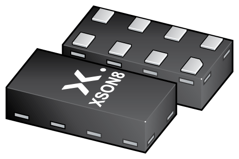
XSON8 (SOT833-1) |
SOT833-1 | SOT833-1_115 |
下表中的所有产品型号均已停产 。
| 型号 | 可订购的器件编号,(订购码(12NC)) | 状态 | 标示 | 封装 | 外形图 | 回流焊/波峰焊 | 包装 |
|---|---|---|---|---|---|---|---|
| 74LVC1G99GD | 74LVC1G99GD,125 (935291883125) |
Obsolete | V99 Standard Procedure Standard Procedure |
XSON8 (SOT996-2) |
SOT996-2 | SOT996-2_125 | |
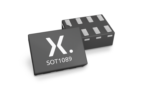
| 74LVC1G99GF | 74LVC1G99GF,115 (935290508115) |
Withdrawn / End-of-life | YF |
XSON8 (SOT1089) |
SOT1089 |
REFLOW_BG-BD-1
|
SOT1089_115 |
| 74LVC1G99GM | 74LVC1G99GM,125 (935284438125) |
Obsolete | V99 |
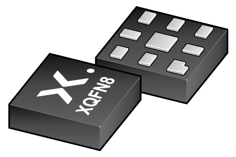
XQFN8 (SOT902-2) |
SOT902-2 | SOT902-2_125 |
环境信息
| 型号 | 可订购的器件编号 | 化学成分 | RoHS | RHF指示符 |
|---|---|---|---|---|
| 74LVC1G99DP | 74LVC1G99DP,125 | 74LVC1G99DP |
|
|
| 74LVC1G99GN | 74LVC1G99GN,115 | 74LVC1G99GN |
|
|
| 74LVC1G99GS | 74LVC1G99GS,115 | 74LVC1G99GS |
|
|
| 74LVC1G99GT | 74LVC1G99GT,115 | 74LVC1G99GT |
|
|
下表中的所有产品型号均已停产 。
| 型号 | 可订购的器件编号 | 化学成分 | RoHS | RHF指示符 |
|---|---|---|---|---|
| 74LVC1G99GD | 74LVC1G99GD,125 | 74LVC1G99GD |
|
|
| 74LVC1G99GF | 74LVC1G99GF,115 | 74LVC1G99GF |
|
|
| 74LVC1G99GM | 74LVC1G99GM,125 | 74LVC1G99GM |
|
|
文档 (29)
| 文件名称 | 标题 | 类型 | 日期 |
|---|---|---|---|
| 74LVC1G99 | Ultra-configurable multiple function gate; 3-state | Data sheet | 2023-08-02 |
| AN11009 | Pin FMEA for LVC family | Application note | 2019-01-09 |
| AN10161 | PicoGate Logic footprints | Application note | 2002-10-29 |
| 001aah322 | Block diagram: 74LVC1G99DP, 74LVC1G99GM, 74LVC1G99GT | Block diagram | 2009-11-03 |
| Nexperia_document_guide_MiniLogic_PicoGate_201901 | PicoGate leaded logic portfolio guide | Brochure | 2019-01-07 |
| Nexperia_document_guide_MiniLogic_MicroPak_201808 | MicroPak leadless logic portfolio guide | Brochure | 2018-09-03 |
| SOT505-2 | 3D model for products with SOT505-2 package | Design support | 2019-01-18 |
| SOT1089 | 3D model for products with SOT1089 package | Design support | 2019-10-07 |
| SOT1116 | 3D model for products with SOT1116 package | Design support | 2023-02-02 |
| SOT1203 | 3D model for products with SOT1203 package | Design support | 2023-02-02 |
| SOT833-1 | 3D model for products with SOT833-1 package | Design support | 2021-01-28 |
| lvc1g99 | 74LVC1G99 IBIS model | IBIS model | 2014-10-20 |
| Nexperia_package_poster | Nexperia package poster | Leaflet | 2020-05-15 |
| XSON8_SOT1089_mk | plastic, extremely thin small outline package; no leads; 8 terminals; 0.55 mm pitch; 1.35 mm x 1 mm x 0.5 mm body | Marcom graphics | 2017-01-28 |
| XQFN8_SOT902-2_mk | plastic, extremely thin quad flat package; 8 terminals; 0.55 mm pitch; 1.6 mm x 1.6 mm x 0.5 mm body | Marcom graphics | 2017-01-28 |
| XSON8_SOT1203_mk | plastic, leadless extremely thin small outline package; 8 terminals; 0.35 mm pitch; 1.35 mm x 1 mm x 0.35 mm body | Marcom graphics | 2019-02-04 |
| SOT505-2 | plastic, thin shrink small outline package; 8 leads; 0.65 mm pitch; 3 mm x 3 mm x 1.1 mm body | Package information | 2022-06-03 |
| SOT996-2 | plastic, leadless extremely thin small outline package; 8 terminals; 0.5 mm pitch; 3 mm x 2 mm x 0.5 mm body | Package information | 2020-04-21 |
| SOT1089 | plastic, leadless extremely thin small outline package; 8 terminals; 0.35 mm pitch; 1.35 mm x 1 mm x 0.5 mm body | Package information | 2022-06-03 |
| SOT902-2 | plastic, leadless extremely thin quad flat package; 8 terminals; 0.5 mm pitch; 1.6 mm x 1.6 mm x 0.5 mm body | Package information | 2020-04-21 |
| SOT1116 | plastic, leadless extremely thin small outline package; 8 terminals; 0.3 mm pitch; 1.2 mm x 1 mm x 0.35 mm body | Package information | 2022-06-02 |
| SOT1203 | plastic, leadless extremely thin small outline package; 8 terminals; 0.35 mm pitch; 1.35 mm x 1 mm x 0.35 mm body | Package information | 2022-06-03 |
| SOT833-1 | plastic, leadless extremely thin small outline package; 8 terminals; 0.5 mm pitch; 1 mm x 1.95 mm x 0.5 mm body | Package information | 2022-06-03 |
| REFLOW_BG-BD-1 | Reflow soldering profile | Reflow soldering | 2021-04-06 |
| Nexperia_Selection_guide_2023 | Nexperia Selection Guide 2023 | Selection guide | 2023-05-10 |
| MAR_SOT1089 | MAR_SOT1089 Topmark | Top marking | 2013-06-03 |
| MAR_SOT1116 | MAR_SOT1116 Topmark | Top marking | 2013-06-03 |
| MAR_SOT1203 | MAR_SOT1203 Topmark | Top marking | 2013-06-03 |
| MAR_SOT833 | MAR_SOT833 Topmark | Top marking | 2013-06-03 |
支持
如果您需要设计/技术支持,请告知我们并填写 应答表 我们会尽快回复您。
模型
| 文件名称 | 标题 | 类型 | 日期 |
|---|---|---|---|
| SOT505-2 | 3D model for products with SOT505-2 package | Design support | 2019-01-18 |
| SOT1089 | 3D model for products with SOT1089 package | Design support | 2019-10-07 |
| SOT1116 | 3D model for products with SOT1116 package | Design support | 2023-02-02 |
| SOT1203 | 3D model for products with SOT1203 package | Design support | 2023-02-02 |
| SOT833-1 | 3D model for products with SOT833-1 package | Design support | 2021-01-28 |
| lvc1g99 | 74LVC1G99 IBIS model | IBIS model | 2014-10-20 |
Ordering, pricing & availability
样品
作为 Nexperia 的客户,您可以通过我们的销售机构订购样品。
如果您没有 Nexperia 的直接账户,我们的全球和地区分销商网络可为您提供 Nexperia 样品支持。查看官方经销商列表。