Register once, drag and drop ECAD models into your CAD tool and speed up your design.
Click here for more information74ALVCH16823DL
18-bit bus-interface D-type flip-flop with reset and enable; 3-state
The 74ALVCH16823 is an 18-bit edge-triggered flip-flop featuring separate D-type inputs for each flip-flop and 3-state outputs for bus oriented applications. Incorporates bushold data inputs which eliminate the need for external pull-up resistors to hold unused inputs. The 74ALVCH16823 consists of two sections of nine edge-triggered flip-flops. A clock (nCP) input, an output-enable (nOE) input, a master reset (nMR) input and a clock-enable (nCE) input are provided for each total 9-bit section.
With the clock-enable (nCE) input LOW, the D-type flip-flops will store the state of their individual nDn-inputs that meet the set-up and hold time requirements on the LOW-to-HIGH nCP transition. Taking nCE HIGH disables the clock buffer, thus latching the outputs. Taking the master reset (nMR) input LOW causes all the nQn outputs to go LOW independently of the clock.
When nOE is LOW, the contents of the flip-flops are available at the outputs. When the nOE is HIGH, the outputs go to the high impedance OFF-state. Operation of the nOE input does not affect the state of flip-flops.
Active bus hold circuitry is provided to hold unused or floating data inputs at a valid logic level.
Features and benefits
Wide supply voltage range from 1.2 V to 3.6 V
CMOS low-power consumption
Direct interface with TTL levels
Current drive ± 24 mA at 3.0 V
MULTIBYTE™ flow-through standard pin-out architecture
Low inductance multiple VCC and GND pins for minimum noise and ground bounce
Output drive capability 50 Ω transmission lines at 85°C
All data inputs have bushold
Complies with JEDEC standard no. 8-1A
Complies with JEDEC standards:
JESD8-5 (2.3 V to 2.7 V)
JESD8B/JESD36 (2.7 V to 3.6 V)
ESD protection:
- HBM: ANSI/ESDA/JEDEC JS-001 class 2 exceeds 2000 V
- CDM: ANSI/ESDA/JEDEC JS-002 class C3 exceeds 1000 V
- Specified from -40 °C to +85 °C
参数类型
| 型号 | Package name |
|---|---|
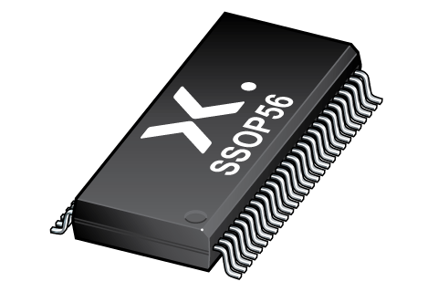
| 74ALVCH16823DL | SSOP56 |
封装
下表中的所有产品型号均已停产 。
| 型号 | 可订购的器件编号,(订购码(12NC)) | 状态 | 标示 | 封装 | 外形图 | 回流焊/波峰焊 | 包装 |
|---|---|---|---|---|---|---|---|
| 74ALVCH16823DL | 74ALVCH16823DL,112 (935259020112) |
Obsolete | ALVCH16823 Standard Procedure Standard Procedure |
SSOP56 (SOT371-1) |
SOT371-1 |
SSOP-TSSOP-VSO-REFLOW
SSOP-TSSOP-VSO-WAVE |
暂无信息 |
| 74ALVCH16823DL,118 (935259020118) |
Obsolete | ALVCH16823 Standard Procedure Standard Procedure | 暂无信息 | ||||
| 74ALVCH16823DL,512 (935259020512) |
Obsolete | ALVCH16823 Standard Procedure Standard Procedure | 暂无信息 | ||||
| 74ALVCH16823DL,518 (935259020518) |
Obsolete | ALVCH16823 Standard Procedure Standard Procedure | 暂无信息 |
环境信息
下表中的所有产品型号均已停产 。
| 型号 | 可订购的器件编号 | 化学成分 | RoHS | RHF指示符 |
|---|---|---|---|---|
| 74ALVCH16823DL | 74ALVCH16823DL,112 | 74ALVCH16823DL |
|
|
| 74ALVCH16823DL | 74ALVCH16823DL,118 | 74ALVCH16823DL |
|
|
| 74ALVCH16823DL | 74ALVCH16823DL,512 | 74ALVCH16823DL |
|
|
| 74ALVCH16823DL | 74ALVCH16823DL,518 | 74ALVCH16823DL |
|
|
Series
文档 (6)
| 文件名称 | 标题 | 类型 | 日期 |
|---|---|---|---|
| 74ALVCH16823 | 18-bit bus-interface D-type flip-flop with reset and enable; 3-state | Data sheet | 2024-07-09 |
| alvch16823 | alvch16823 IBIS model | IBIS model | 2013-04-08 |
| Nexperia_package_poster | Nexperia package poster | Leaflet | 2020-05-15 |
| SOT371-1 | plastic, shrink small outline package; 56 leads; 0.635 mm pitch; 18.45 mm x 7.5 mm x 2.8 mm body | Package information | 2020-04-21 |
| SSOP-TSSOP-VSO-REFLOW | Footprint for reflow soldering | Reflow soldering | 2009-10-08 |
| SSOP-TSSOP-VSO-WAVE | Footprint for wave soldering | Wave soldering | 2009-10-08 |
支持
如果您需要设计/技术支持,请告知我们并填写 应答表 我们会尽快回复您。
模型
| 文件名称 | 标题 | 类型 | 日期 |
|---|---|---|---|
| alvch16823 | alvch16823 IBIS model | IBIS model | 2013-04-08 |
How does it work?
The interactive datasheets are based on the Nexperia MOSFET precision electrothermal models. With our interactive datasheets you can simply specify your own conditions interactively. Start by changing the values of the conditions. You can do this by using the sliders in the condition fields. By dragging the sliders you will see how the MOSFET will perform at the new conditions set.
74ALVCH16823DL
18-bit bus-interface D-type flip-flop with reset and enable; 3-state
从安世半导体购买
| SKU | 库存* | MOQ | 单位价格 | 数量 |
|---|