
74AVC16T245
16-bit dual supply translating transceiver with configurable voltage translation; 3-state
The 74AVC16T245 is a 16-bit transceiver with bidirectional level voltage translation and 3-state outputs. The device can be used as two 8-bit transceivers or as a 16-bit transceiver. It has dual supplies (VCC(A) and VCC(B)) for voltage translation and four 8-bit input-output ports (nAn and nBn) each with its own output enable (nOE) and send/receive (nDIR) input for direction control. VCC(A) and VCC(B) can be independently supplied at any voltage between 0.8 V and 3.6 V making the device suitable for low voltage translation between any of the following voltages: 0.8 V, 1.2 V, 1.5 V, 1.8 V, 2.5 V and 3.3 V. A HIGH on nDIR selects transmission from nAn to nBn while a LOW on nDIR selects transmission from nBn to nAn. A HIGH on nOE causes the outputs to assume a high-impedance OFF-state
The device is fully specified for partial power-down applications using IOFF. The IOFF circuitry disables the output, preventing any damaging backflow current through the device when it is powered down. In suspend mode when either VCC(A) or VCC(B) are at GND level, both nAn and nBn are in the high-impedance OFF-state.
Features and benefits
Wide supply voltage range:
VCC(A): 0.8 V to 3.6 V
VCC(B): 0.8 V to 3.6 V
Complies with JEDEC standards:
JESD8-12 (0.8 V to 1.3 V)
JESD8-11 (0.9 V to 1.65 V)
JESD8-7 (1.2 V to 1.95 V)
JESD8-5 (1.8 V to 2.7 V)
JESD8-B (2.7 V to 3.6 V)
Maximum data rates:
380 Mbit/s (≥ 1.8 V to 3.3 V translation)
200 Mbit/s (≥ 1.1 V to 3.3 V translation)
200 Mbit/s (≥ 1.1 V to 2.5 V translation)
200 Mbit/s (≥ 1.1 V to 1.8 V translation)
150 Mbit/s (≥ 1.1 V to 1.5 V translation)
100 Mbit/s (≥ 1.1 V to 1.2 V translation)
Suspend mode
Latch-up performance exceeds 100 mA per JESD 78 Class II
Inputs accept voltages up to 3.6 V
IOFF circuitry provides partial Power-down mode operation
ESD protection:
HBM: ANSI/ESDA/JEDEC JS-001 class 3B exceeds 8000 V
CDM: ANSI/ESDA/JEDEC JS-002 class C3 exceeds 1000 V
Specified from -40 °C to +85 °C and -40 °C to +125 °C
参数类型
| 型号 | VCC(A) (V) | VCC(B) (V) | Logic switching levels | Output drive capability (mA) | tpd (ns) | Nr of bits | Power dissipation considerations | Tamb (°C) | Package name |
|---|---|---|---|---|---|---|---|---|---|
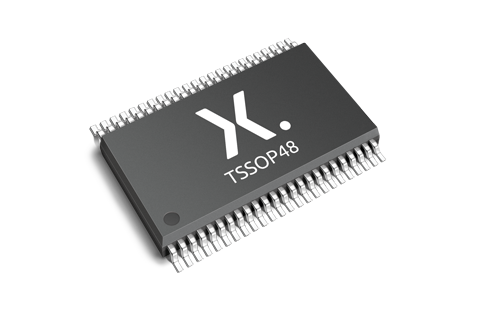
| 74AVC16T245DGG | 0.8 - 3.6 | 0.8 - 3.6 | CMOS/LVTTL | ± 12 | 2.1 | 16 | very low | -40~125 | TSSOP48 |
| 74AVC16T245DGV | 0.8 - 3.6 | 0.8 - 3.6 | CMOS/LVTTL | ± 12 | 2.1 | 16 | very low | -40~125 | TVSOP48 |
封装
| 型号 | 可订购的器件编号,(订购码(12NC)) | 状态 | 标示 | 封装 | 外形图 | 回流焊/波峰焊 | 包装 |
|---|---|---|---|---|---|---|---|
| 74AVC16T245DGG | 74AVC16T245DGG,118 (935286228118) |
Active | AVC16T245 |
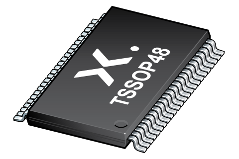
TSSOP48 (SOT362-1) |
SOT362-1 |
SSOP-TSSOP-VSO-WAVE
|
SOT362-1_118 |
| 74AVC16T245DGV | 74AVC16T245DGV,118 (935288133118) |
Active | AVC16T245 |
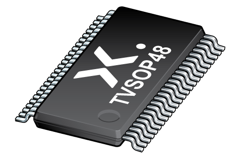
TVSOP48 (SOT480-1) |
SOT480-1 | SOT480-1_118 |
下表中的所有产品型号均已停产 。
| 型号 | 可订购的器件编号,(订购码(12NC)) | 状态 | 标示 | 封装 | 外形图 | 回流焊/波峰焊 | 包装 |
|---|---|---|---|---|---|---|---|
| 74AVC16T245BX | 74AVC16T245BX,518 (935295866518) |
Obsolete | AVC16T245 Standard Procedure Standard Procedure | no package information | |||
| 74AVC16T245EV | 74AVC16T245EVY (935288136518) |
Obsolete | AVC16T245 | no package information | |||
| 74AVC16T245EV,551 (935288136551) |
Obsolete | AVC16T245 | |||||
| 74AVC16T245EV,557 (935288136557) |
Obsolete | AVC16T245 | |||||
环境信息
| 型号 | 可订购的器件编号 | 化学成分 | RoHS | RHF指示符 |
|---|---|---|---|---|
| 74AVC16T245DGG | 74AVC16T245DGG,118 | 74AVC16T245DGG |
|
|
| 74AVC16T245DGV | 74AVC16T245DGV,118 | 74AVC16T245DGV |
|
|
下表中的所有产品型号均已停产 。
| 型号 | 可订购的器件编号 | 化学成分 | RoHS | RHF指示符 |
|---|---|---|---|---|
| 74AVC16T245BX | 74AVC16T245BX,518 | 74AVC16T245BX |
|
|
| 74AVC16T245EV | 74AVC16T245EVY | 74AVC16T245EV |
|
|
| 74AVC16T245EV | 74AVC16T245EV,551 | 74AVC16T245EV |
|
|
| 74AVC16T245EV | 74AVC16T245EV,557 | 74AVC16T245EV |
|
文档 (13)
| 文件名称 | 标题 | 类型 | 日期 |
|---|---|---|---|
| 74AVC16T245 | 16-bit dual supply translating transceiver with configurable voltage translation; 3-state | Data sheet | 2024-06-25 |
| 001aak425 | Block diagram: 74AVC16T245DGV, 74AVCH16T245BQ, 74AVCH16T245DGG | Block diagram | 2009-11-03 |
| 001aak426 | Block diagram: 74AVC16T245DGV, 74AVCH16T245BQ, 74AVCH16T245DGG | Block diagram | 2009-11-04 |
| SOT362-1 | 3D model for products with SOT362-1 package | Design support | 2020-01-22 |
| SOT480-1 | 3D model for products with SOT480-1 package | Design support | 2020-01-22 |
| avc16t245 | AVC16T245 IBIS model | IBIS model | 2013-05-06 |
| Nexperia_package_poster | Nexperia package poster | Leaflet | 2020-05-15 |
| Nexperia_document_leaflet_Logic_TVSOP48_16bitPortfolio_201903 | Smaller-footprint 16-bit logic with advanced features | Leaflet | 2019-03-29 |
| TSSOP48_SOT362-1_mk | plastic, thin shrink small outline package; 48 leads; 0.5 mm pitch; 12.8 mm x 6.1 mm x 1.2 mm body | Marcom graphics | 2017-01-28 |
| SOT362-1 | plastic thin shrink small outline package; 48 leads; body width 6.1 mm | Package information | 2024-01-05 |
| SOT480-1 | plastic, thin shrink small outline package; 48 leads; 0.4 mm pitch; 9.7 mm x 4.4 mm x 1.1 mm body | Package information | 2022-06-22 |
| Nexperia_Selection_guide_2023 | Nexperia Selection Guide 2023 | Selection guide | 2023-05-10 |
| SSOP-TSSOP-VSO-WAVE | Footprint for wave soldering | Wave soldering | 2009-10-08 |
支持
如果您需要设计/技术支持,请告知我们并填写 应答表 我们会尽快回复您。
Ordering, pricing & availability
样品
作为 Nexperia 的客户,您可以通过我们的销售机构订购样品。
如果您没有 Nexperia 的直接账户,我们的全球和地区分销商网络可为您提供 Nexperia 样品支持。查看官方经销商列表。