Register once, drag and drop ECAD models into your CAD tool and speed up your design.
Click here for more information74AUP1T1326GT
Low-power dual supply buffer/line driver; 3-state
The 74AUP1T1326 is a high-performance, low-power, low-voltage, single-bit, dual supply buffer/line driver with output enable circuitry. The 74AUP1T1326 is designed for logic-level translation applications and combines the functions of the 74AUP1G32 and 74AUP1G126. The buffer/line driver is controlled by two output enable Schmitt trigger inputs (1OE and 2OE) through an OR-gate. The output enable inputs accept standard input signals and are capable of transforming slowly changing input signals into sharply defined, jitter-free output signals. The output of the OR-gate is also available at output 1Y.
Features and benefits
- Complies with JEDEC standard: JESD8-5 (1.8 V to 2.7 V)
- Complies with JEDEC standard: JESD8-7 (1.2 V to 1.95 V)
- Complies with JEDEC standard: JESD8-B (2.7 V to 3.6 V)
- ESD protection: CDM JESD22-C101C exceeds 1000 V
- ESD protection: HBM JESD22-A114E Class 2A exceeds 2000 V
- ESD protection: MM JESD22-A115-A exceeds 200 V
- High noise immunity
- IOFF circuitry provides partial Power-down mode operation
- Inputs accept voltages up to 3.6 V
- Latch-up performance exceeds 100 mA per JESD 78 Class II
- Low noise overshoot and undershoot < 10 % of VCC
- Low static power consumption; ICC = 0.9 μA (maximu)
- Multiple package options
- Specified from 40 °C to +85 °C
- Wide supply voltage range: VCC(A): 1.1 V to 3.6 V
- Wide supply voltage range: VCC(B): 1.1 V to 3.6 V
Applications
Parametrics
| Type number | Package name |
|---|---|
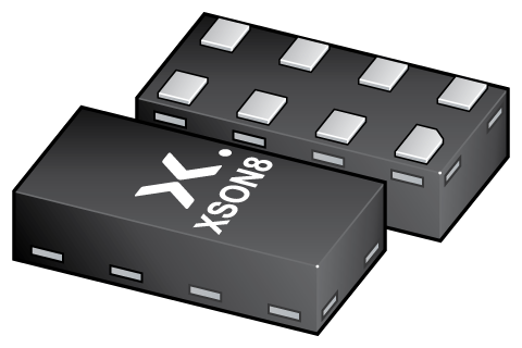
| 74AUP1T1326GT | XSON8 |
Package
All type numbers in the table below are discontinued.
| Type number | Orderable part number, (Ordering code (12NC)) | Status | Marking | Package | Package information | Reflow-/Wave soldering | Packing |
|---|---|---|---|---|---|---|---|
| 74AUP1T1326GT | 74AUP1T1326GT,115 (935286082115) |
Obsolete | p31 |

XSON8 (SOT833-1) |
SOT833-1 | SOT833-1_115 |
Environmental information
All type numbers in the table below are discontinued.
| Type number | Orderable part number | Chemical content | RoHS | RHF-indicator |
|---|---|---|---|---|
| 74AUP1T1326GT | 74AUP1T1326GT,115 | 74AUP1T1326GT |
|
|
Series
Documentation (8)
| File name | Title | Type | Date |
|---|---|---|---|
| 74AUP1T1326 | Low-power dual supply buffer/line driver; 3-state | Data sheet | 2018-07-23 |
| AN10161 | PicoGate Logic footprints | Application note | 2002-10-29 |
| Nexperia_document_guide_MiniLogic_MicroPak_201808 | MicroPak leadless logic portfolio guide | Brochure | 2018-09-03 |
| SOT833-1 | 3D model for products with SOT833-1 package | Design support | 2021-01-28 |
| Nexperia_document_leaflet_Logic_AUP_technology_portfolio_201904 | Nexperia_document_leaflet_Logic_AUP_technology_portfolio_201904 | Leaflet | 2019-04-12 |
| Nexperia_package_poster | Nexperia package poster | Leaflet | 2020-05-15 |
| SOT833-1 | plastic, leadless extremely thin small outline package; 8 terminals; 0.5 mm pitch; 1 mm x 1.95 mm x 0.5 mm body | Package information | 2022-06-03 |
| MAR_SOT833 | MAR_SOT833 Topmark | Top marking | 2013-06-03 |
Support
If you are in need of design/technical support, let us know and fill in the answer form we'll get back to you shortly.
Longevity
The Nexperia Longevity Program is aimed to provide our customers information from time to time about the expected time that our products can be ordered. The NLP is reviewed and updated regularly by our Executive Management Team. View our longevity program here.
Models
| File name | Title | Type | Date |
|---|---|---|---|
| SOT833-1 | 3D model for products with SOT833-1 package | Design support | 2021-01-28 |
How does it work?
The interactive datasheets are based on the Nexperia MOSFET precision electrothermal models. With our interactive datasheets you can simply specify your own conditions interactively. Start by changing the values of the conditions. You can do this by using the sliders in the condition fields. By dragging the sliders you will see how the MOSFET will perform at the new conditions set.