Register once, drag and drop ECAD models into your CAD tool and speed up your design.
Click here for more information74LV02D
Quad 2-input NOR gate
The 74LV02 is a low-voltage Si-gate CMOS device that is pin and function compatible with 74HC02 and 74HCT02.
The 74LV02 provides a quad 2-input NOR function.
Features and benefits
Wide operating voltage: 1.0 V to 5.5 V
Optimized for low voltage applications: 1.0 V to 3.6 V
Accepts TTL input levels between VCC = 2.7 V and VCC = 3.6 V
Typical output ground bounce < 0.8 V at VCC = 3.3 V and Tamb = 25 °C
Typical HIGH-level output voltage (VOH) undershoot: > 2 V at VCC = 3.3 V and Tamb = 25 °C
ESD protection:
HBM JESD22-A114E exceeds 2000 V
MM JESD22-A115-A exceeds 200 V
Multiple package options
Specified from -40 °C to +85 °C and from -40 °C to +125 °C
Applications
Parametrics
| Type number | Package name |
|---|---|
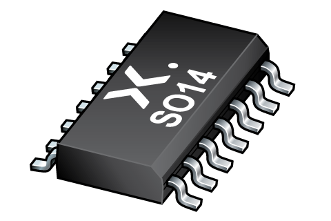
| 74LV02D | SO14 |
PCB Symbol, Footprint and 3D Model
| Model Name | Description |
|---|---|
|
|
Package
All type numbers in the table below are discontinued.
| Type number | Orderable part number, (Ordering code (12NC)) | Status | Marking | Package | Package information | Reflow-/Wave soldering | Packing |
|---|---|---|---|---|---|---|---|
| 74LV02D | 74LV02D,118 (935063110118) |
Withdrawn / End-of-life |

SO14 (SOT108-1) |
SOT108-1 |
SO-SOJ-REFLOW
SO-SOJ-WAVE WAVE_BG-BD-1 |
SOT108-1_118 | |
| 74LV02D,112 (935063110112) |
Obsolete | SOT108-1_112 |
Environmental information
All type numbers in the table below are discontinued.
| Type number | Orderable part number | Chemical content | RoHS | RHF-indicator |
|---|---|---|---|---|
| 74LV02D | 74LV02D,118 | 74LV02D |
|
|
| 74LV02D | 74LV02D,112 | 74LV02D |
|
|
Documentation (10)
| File name | Title | Type | Date |
|---|---|---|---|
| 74LV02 | Quad 2-input NOR gate | Data sheet | 2017-05-10 |
| AN90063 | Questions about package outline drawings | Application note | 2025-03-12 |
| SOT108-1 | 3D model for products with SOT108-1 package | Design support | 2020-01-22 |
| lv02 | 74LV02 IBIS model | IBIS model | 2019-01-09 |
| Nexperia_package_poster | Nexperia package poster | Leaflet | 2020-05-15 |
| SO14_SOT108-1_mk | plastic, small outline package; 14 leads; 1.27 mm pitch; 8.65 mm x 3.9 mm x 1.75 mm body | Marcom graphics | 2017-01-28 |
| SOT108-1 | plastic, small outline package; 14 leads; 1.27 mm pitch; 8.65 mm x 3.9 mm x 1.75 mm body | Package information | 2023-11-07 |
| SO-SOJ-REFLOW | Footprint for reflow soldering | Reflow soldering | 2009-10-08 |
| SO-SOJ-WAVE | Footprint for wave soldering | Wave soldering | 2009-10-08 |
| WAVE_BG-BD-1 | Wave soldering profile | Wave soldering | 2021-09-08 |
Support
If you are in need of design/technical support, let us know and fill in the answer form we'll get back to you shortly.
Longevity
The Nexperia Longevity Program is aimed to provide our customers information from time to time about the expected time that our products can be ordered. The NLP is reviewed and updated regularly by our Executive Management Team. View our longevity program here.
PCB Symbol, Footprint and 3D Model
| Model Name | Description |
|---|---|
|
|
How does it work?
The interactive datasheets are based on the Nexperia MOSFET precision electrothermal models. With our interactive datasheets you can simply specify your own conditions interactively. Start by changing the values of the conditions. You can do this by using the sliders in the condition fields. By dragging the sliders you will see how the MOSFET will perform at the new conditions set.