Register once, drag and drop ECAD models into your CAD tool and speed up your design.
Click here for more information74LV4051DB
8-channel analog multiplexer/demultiplexer
The 74LV4051 is an 8-channel analog multiplexer/demultiplexer with three digital select inputs (S0 to S2), an active-LOW enable input (E), eight independent inputs/outputs (Y0 to Y7) and a common input/output (Z). It is a low-voltage Si-gate CMOS device that is pin and function compatible with 74HC4051 and 74HCT4051. With E LOW, one of the eight switches is selected (low impedance ON-state) by S0 to S2. With E HIGH, all switches are in the high-impedance OFF-state, independent of S0 to S2.
VCC and GND are the supply voltage pins for the digital control inputs (S0 to S2, and E). The VCC to GND ranges are 1.0 V to 6.0 V. The analog inputs/outputs (Y0 to Y7, and Z) can swing between VCC as a positive limit and VEE as a negative limit. VCC - VEE may not exceed 6.0 V. For operation as a digital multiplexer/demultiplexer, VEE is connected to GND (typically ground).
Alternatives
Features and benefits
Optimized for low-voltage applications: 1.0 V to 6.0 V
Accepts TTL input levels between VCC = 2.7 V and VCC = 3.6 V
Low ON resistance:
145 Ω (typical) at VCC - VEE = 2.0 V
80 Ω (typical) at VCC - VEE = 3.0 V
60 Ω (typical) at VCC - VEE = 4.5 V
Logic level translation:
To enable 3 V logic to communicate with ±3 V analog signals
Typical ‘break before make’ built in
ESD protection:
HBM: ANSI/ESDA/JEDEC JS-001 class 2 exceeds 2000 V
CDM: ANSI/ESDA/JEDEC JS-002 class C3 exceeds 1000 V
Multiple package options
Specified from -40 °C to +85 °C and from -40 °C to +125 °C
Parametrics
| Type number | Package name |
|---|---|
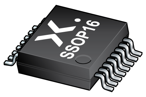
| 74LV4051DB | SSOP16 |
PCB Symbol, Footprint and 3D Model
| Model Name | Description |
|---|---|
|
|
Package
All type numbers in the table below are discontinued.
| Type number | Orderable part number, (Ordering code (12NC)) | Status | Marking | Package | Package information | Reflow-/Wave soldering | Packing |
|---|---|---|---|---|---|---|---|
| 74LV4051DB | 74LV4051DB,112 (935190980112) |
Obsolete | LV4051 |

SSOP16 (SOT338-1) |
SOT338-1 |
SSOP-TSSOP-VSO-REFLOW
SSOP-TSSOP-VSO-WAVE |
Not available |
| 74LV4051DB,118 (935190980118) |
Obsolete | LV4051 | Not available |
Environmental information
All type numbers in the table below are discontinued.
| Type number | Orderable part number | Chemical content | RoHS | RHF-indicator |
|---|---|---|---|---|
| 74LV4051DB | 74LV4051DB,112 | 74LV4051DB |
|
|
| 74LV4051DB | 74LV4051DB,118 | 74LV4051DB |
|
|
Series
Documentation (7)
| File name | Title | Type | Date |
|---|---|---|---|
| 74LV4051 | 8-channel analog multiplexer/demultiplexer | Data sheet | 2024-03-29 |
| Nexperia_package_poster | Nexperia package poster | Leaflet | 2020-05-15 |
| SSOP16_SOT338-1_mk | plastic, shrink small outline package; 16 leads; 0.65 mm pitch; 6.2 mm x 5.3 mm x 2 mm body | Marcom graphics | 2017-01-28 |
| SOT338-1 | plastic, shrink small outline package; 16 leads; 0.65 mm pitch; 6.2 mm x 5.3 mm x 2 mm body | Package information | 2022-06-20 |
| SSOP-TSSOP-VSO-REFLOW | Footprint for reflow soldering | Reflow soldering | 2009-10-08 |
| lv | lv Spice model | SPICE model | 2013-05-07 |
| SSOP-TSSOP-VSO-WAVE | Footprint for wave soldering | Wave soldering | 2009-10-08 |
Support
If you are in need of design/technical support, let us know and fill in the answer form we'll get back to you shortly.
Longevity
The Nexperia Longevity Program is aimed to provide our customers information from time to time about the expected time that our products can be ordered. The NLP is reviewed and updated regularly by our Executive Management Team. View our longevity program here.
Models
| File name | Title | Type | Date |
|---|---|---|---|
| lv | lv Spice model | SPICE model | 2013-05-07 |
PCB Symbol, Footprint and 3D Model
| Model Name | Description |
|---|---|
|
|
How does it work?
The interactive datasheets are based on the Nexperia MOSFET precision electrothermal models. With our interactive datasheets you can simply specify your own conditions interactively. Start by changing the values of the conditions. You can do this by using the sliders in the condition fields. By dragging the sliders you will see how the MOSFET will perform at the new conditions set.
