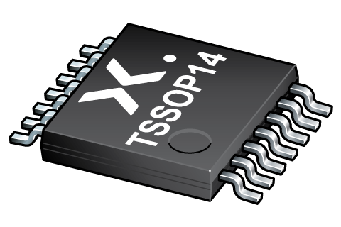
Orderable parts
| Type number | Orderable part number | Ordering code (12NC) | Package | Buy from distributors |
|---|---|---|---|---|
| HEF4013BTT | HEF4013BTT,118 | 935283039118 | SOT402-1 | Order product |

Register once, drag and drop ECAD models into your CAD tool and speed up your design.
Click here for more informationDual D-type flip-flop
The HEF4013B is a dual D-type flip-flop with set and reset; positive-edge trigger. Inputs include clamp diodes. This enables the use of current limiting resistors to interface inputs to voltages in excess of VDD. Schmitt-trigger action on the clock input makes the circuit highly tolerant of slower clock rise and fall times.
Wide supply voltage range from 3.0 V to 15.0 V
CMOS low power dissipation
High noise immunity
Tolerant of slow clock rise and fall times
Fully static operation
5 V, 10 V, and 15 V parametric ratings
Standardized symmetrical output characteristics
Specified from -40 °C to +125 °C
Complies with JEDEC standard JESD 13-B
HBM: ANSI/ESDA/JEDEC JS-001 class 2 exceeds 2000 V
CDM: ANSI/ESDA/JEDEC JS-002 class C3 exceeds 1000 V
Counters and dividers
Registers
Toggle flip-flops
| Type number | VCC (V) | Logic switching levels | Output drive capability (mA) | tpd (ns) | fmax (MHz) | Power dissipation considerations | Tamb (°C) | Rth(j-a) (K/W) | Ψth(j-top) (K/W) | Rth(j-c) (K/W) | Package name |
|---|---|---|---|---|---|---|---|---|---|---|---|
| HEF4013BTT | 3.0 - 15 | CMOS | ± 2.4 | 30 | 40 | low | -40~85 | 139 | 7.1 | 65 | TSSOP14 |
| Model Name | Description |
|---|---|
|
|
| Type number | Orderable part number, (Ordering code (12NC)) | Status | Marking | Package | Package information | Reflow-/Wave soldering | Packing |
|---|---|---|---|---|---|---|---|
| HEF4013BTT | HEF4013BTT,118 (935283039118) |
Active | EF4013B |

TSSOP14 (SOT402-1) |
SOT402-1 |
SSOP-TSSOP-VSO-WAVE
|
SOT402-1_118 |
| Type number | Orderable part number | Chemical content | RoHS | RHF-indicator |
|---|---|---|---|---|
| HEF4013BTT | HEF4013BTT,118 | HEF4013BTT |
|
|
| File name | Title | Type | Date |
|---|---|---|---|
| HEF4013B | Dual D-type flip-flop | Data sheet | 2024-07-24 |
| AN11051 | Pin FMEA HEF4000 family | Application note | 2019-01-09 |
| SOT402-1 | 3D model for products with SOT402-1 package | Design support | 2023-02-02 |
| Nexperia_package_poster | Nexperia package poster | Leaflet | 2020-05-15 |
| TSSOP14_SOT402-1_mk | plastic, thin shrink small outline package; 14 leads; 0.65 mm pitch; 5 mm x 4.4 mm x 1.1 mm body | Marcom graphics | 2017-01-28 |
| SOT402-1 | plastic, thin shrink small outline package; 14 leads; 0.65 mm pitch; 5 mm x 4.4 mm x 1.2 mm body | Package information | 2023-11-07 |
| SOT402-1_118 | TSSOP14; Reel pack for SMD, 13"; Q1/T1 product orientation | Packing information | 2025-01-16 |
| HEF4013BTT_Nexperia_Product_Reliability | HEF4013BTT Nexperia Product Reliability | Quality document | 2025-03-20 |
| SSOP-TSSOP-VSO-WAVE | Footprint for wave soldering | Wave soldering | 2009-10-08 |
If you are in need of design/technical support, let us know and fill in the answer form we'll get back to you shortly.
The Nexperia Longevity Program is aimed to provide our customers information from time to time about the expected time that our products can be ordered. The NLP is reviewed and updated regularly by our Executive Management Team. View our longevity program here.
| File name | Title | Type | Date |
|---|---|---|---|
| SOT402-1 | 3D model for products with SOT402-1 package | Design support | 2023-02-02 |
| Model Name | Description |
|---|---|
|
|
| Type number | Orderable part number | Ordering code (12NC) | Status | Packing | Packing Quantity | Buy online |
|---|---|---|---|---|---|---|
| HEF4013BTT | HEF4013BTT,118 | 935283039118 | Active | SOT402-1_118 | 2,500 |
|
As a Nexperia customer you can order samples via our sales organization.
If you do not have a direct account with Nexperia our network of global and regional distributors is available and equipped to support you with Nexperia samples. Check out the list of official distributors.
The interactive datasheets are based on the Nexperia MOSFET precision electrothermal models. With our interactive datasheets you can simply specify your own conditions interactively. Start by changing the values of the conditions. You can do this by using the sliders in the condition fields. By dragging the sliders you will see how the MOSFET will perform at the new conditions set.