Register once, drag and drop ECAD models into your CAD tool and speed up your design.
Click here for more informationPDI1284P11DGG
3.3 V parallel interface transceiver/buffer
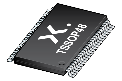
The PDI1284P11 parallel interface chip is designed to provide an asynchronous, 8-bit, bidirectional, parallel interface for personal computers. The PDI1284P11 includes all 19 signal lines defined by the IEEE 1284 interface specification for Byte, Nibble, EPP, and ECP modes. The PDI1284P11 is designed for hosts or peripherals operating at 3.3 V to interface 3.3 V or 5.0 V devices.
The eight transceiver pairs (A/B 1 to 8) allow data transmission from the A-bus to the B-bus, or from the B-bus to the A-bus, depending on the state of the direction pin DIR.
The B-bus and the Y9 to Y13 lines have either totem pole or resistor pull-up outputs, depending on the state of the high drive enable pin HD. The A-bus has only totem pole style outputs. All inputs are TTL compatible with at least 400 mV of input hysteresis at VCC = 3.3 V.
Features and benefits
Asynchronous operation
8-bit transceivers
Six additional buffer/driver lines peripheral to cable
Five additional control lines from cable
5 V tolerant
ESD protection:
HBM JESD22-A114E exceeds 2000 V
MM JESD22-A115-A exceeds 200 V
Latch-up current protection exceeds 500 mA per JEDEC Std 19
Input hysteresis
Low-noise operation
IEEE 1284 compliant level 1 and 2
Overvoltage protection on B/Y side for off-state
A side 3-state option
B side active or resistive pull-up option
Cable side supply voltage for 5 V or 3 V operation
Parametrics
| Type number | Package name |
|---|---|
| PDI1284P11DGG | TSSOP48 |
PCB Symbol, Footprint and 3D Model
| Model Name | Description |
|---|---|
|
|
Package
All type numbers in the table below are discontinued.
| Type number | Orderable part number, (Ordering code (12NC)) | Status | Marking | Package | Package information | Reflow-/Wave soldering | Packing |
|---|---|---|---|---|---|---|---|
| PDI1284P11DGG | PDI1284P11DGG,112 (935223080112) |
Obsolete | PDI1284P11DGG PDI1284P11DGG Standard Procedure Standard Procedure |

TSSOP48 (SOT362-1) |
SOT362-1 |
SSOP-TSSOP-VSO-WAVE
|
Not available |
| PDI1284P11DGG,118 (935223080118) |
Obsolete | PDI1284P11DGG PDI1284P11DGG Standard Procedure Standard Procedure | SOT362-1_118 | ||||
| PDI1284P11DGG,698 (935223080698) |
Obsolete | PDI1284P11DGG PDI1284P11DGG Standard Procedure Standard Procedure | Not available |
Environmental information
All type numbers in the table below are discontinued.
Series
Documentation (8)
| File name | Title | Type | Date |
|---|---|---|---|
| PDI1284P11 | 3.3 V parallel interface transceiver/buffer | Data sheet | 2021-07-06 |
| AN263 | Power considerations when using CMOS and BiCMOS logic devices | Application note | 2023-02-07 |
| SOT362-1 | 3D model for products with SOT362-1 package | Design support | 2020-01-22 |
| Nexperia_package_poster | Nexperia package poster | Leaflet | 2020-05-15 |
| TSSOP48_SOT362-1_mk | plastic, thin shrink small outline package; 48 leads; 0.5 mm pitch; 12.8 mm x 6.1 mm x 1.2 mm body | Marcom graphics | 2017-01-28 |
| SOT362-1 | plastic thin shrink small outline package; 48 leads; body width 6.1 mm | Package information | 2024-01-05 |
| PDI1284P11DGG_Nexperia_Product_Reliability | PDI1284P11DGG Nexperia Product Reliability | Quality document | 2022-05-04 |
| SSOP-TSSOP-VSO-WAVE | Footprint for wave soldering | Wave soldering | 2009-10-08 |
Support
If you are in need of design/technical support, let us know and fill in the answer form we'll get back to you shortly.
Longevity
The Nexperia Longevity Program is aimed to provide our customers information from time to time about the expected time that our products can be ordered. The NLP is reviewed and updated regularly by our Executive Management Team. View our longevity program here.
Models
| File name | Title | Type | Date |
|---|---|---|---|
| SOT362-1 | 3D model for products with SOT362-1 package | Design support | 2020-01-22 |
PCB Symbol, Footprint and 3D Model
| Model Name | Description |
|---|---|
|
|
How does it work?
The interactive datasheets are based on the Nexperia MOSFET precision electrothermal models. With our interactive datasheets you can simply specify your own conditions interactively. Start by changing the values of the conditions. You can do this by using the sliders in the condition fields. By dragging the sliders you will see how the MOSFET will perform at the new conditions set.