Register once, drag and drop ECAD models into your CAD tool and speed up your design.
Click here for more informationPMFPB6532UP
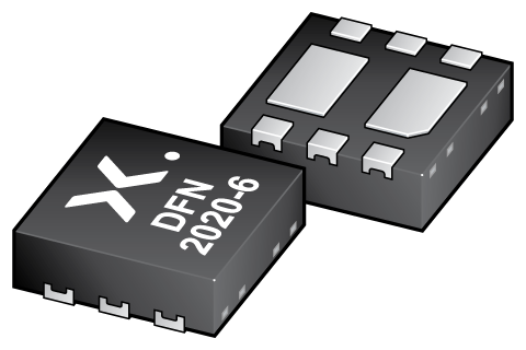
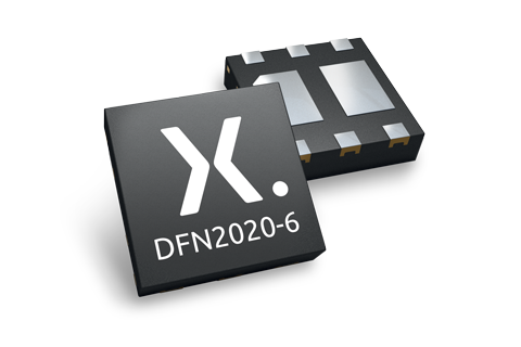
20 V, 3.5 A / 320 mV VF P-channel MOSFET-Schottky combination
Small-signal P-channel enhancement mode Field-Effect Transistor (FET) using Trench MOSFET technology and ultra low VF Maximum Efficiency General Application (MEGA) Schottky diode combined in a small and leadless ultra thin SOT1118 Surface-Mounted Device (SMD) plastic package.
Features and benefits
- Trench MOSFET technology
- Integrated ultra low VF MEGA Schottky diode
- 1 kV ElectroStatic Discharge (ESD) protection
- Small and leadless ultra thin SMD plastic package: 2 × 2 × 0.65 mm
- Exposed drain pad for excellent thermal conduction
Applications
- Charging switch for portable devices
- DC-to-DC converters
- Power management in battery-driven portables
- Hard disk and computing power management
Parametrics
| Type number | Package version | Package name | Product status | Release date |
|---|---|---|---|---|
| PMFPB6532UP | SOT1118 | DFN2020-6 | End of life | 2010-05-03 |
Package
All type numbers in the table below are discontinued.
| Type number | Orderable part number, (Ordering code (12NC)) | Status | Marking | Package | Package information | Reflow-/Wave soldering | Packing |
|---|---|---|---|---|---|---|---|
| PMFPB6532UP | PMFPB6532UP,115 (934064007115) |
Obsolete |
DFN2020-6 (SOT1118) |
SOT1118 |
REFLOW_BG-BD-1
|
SOT1118_115 |
Environmental information
All type numbers in the table below are discontinued.
| Type number | Orderable part number | Chemical content | RoHS | RHF-indicator |
|---|---|---|---|---|
| PMFPB6532UP | PMFPB6532UP,115 | PMFPB6532UP |
|
|
Documentation (18)
| File name | Title | Type | Date |
|---|---|---|---|
| PMFPB6532UP | P-channel MOSFET-Schottky combination | Data sheet | 2012-06-13 |
| AN10273 | Power MOSFET single-shot and repetitive avalanche ruggedness rating | Application note | 2022-06-20 |
| AN10874_ZH | LFPAK MOSFET thermal design guide, Chinese version | Application note | 2020-04-30 |
| AN10910 | Protecting charger interfaces and typical battery charging topologies with external bypass transistors | Application note | 2021-04-12 |
| AN11113_ZH | LFPAK MOSFET thermal design guide - Part 2 | Application note | 2020-04-30 |
| AN11158 | Understanding power MOSFET data sheet parameters | Application note | 2025-02-18 |
| AN11158_ZH | Understanding power MOSFET data sheet parameters | Application note | 2021-01-04 |
| AN11243 | Failure signature of Electrical Overstress on Power MOSFETs | Application note | 2025-03-20 |
| AN11261 | RC Thermal Models | Application note | 2021-03-18 |
| AN11599 | Using power MOSFETs in parallel | Application note | 2016-07-13 |
| AN90063 | Questions about package outline drawings | Application note | 2025-03-12 |
| SOT1118 | 3D model for products with SOT1118 package | Design support | 2019-10-07 |
| Nexperia_package_poster | Nexperia package poster | Leaflet | 2020-05-15 |
| DFN2020-6_SOT1118_mk | plastic, thermal enhanced ultra thin small outline package; no leads; 6 terminals; 0.65 mm pitch; 2 mm x 2 mm x 0.65 mm body | Marcom graphics | 2017-01-28 |
| SOT1118 | plastic, leadless thermal enhanced ultra thin small outline package; no leads; 6 terminals; 0.65 mm pitch; 2 mm x 2 mm x 0.65 mm body | Package information | 2022-06-02 |
| REFLOW_BG-BD-1 | Reflow soldering profile | Reflow soldering | 2021-04-06 |
| PMFPB6532UP_8_20_2010 | PMFPB6532UP Spice model | SPICE model | 2013-12-13 |
| TN00008 | Power MOSFET frequently asked questions and answers | Technical note | 2024-08-09 |
Support
If you are in need of design/technical support, let us know and fill in the answer form we'll get back to you shortly.
Longevity
The Nexperia Longevity Program is aimed to provide our customers information from time to time about the expected time that our products can be ordered. The NLP is reviewed and updated regularly by our Executive Management Team. View our longevity program here.
Models
| File name | Title | Type | Date |
|---|---|---|---|
| PMFPB6532UP_8_20_2010 | PMFPB6532UP Spice model | SPICE model | 2013-12-13 |
| SOT1118 | 3D model for products with SOT1118 package | Design support | 2019-10-07 |
How does it work?
The interactive datasheets are based on the Nexperia MOSFET precision electrothermal models. With our interactive datasheets you can simply specify your own conditions interactively. Start by changing the values of the conditions. You can do this by using the sliders in the condition fields. By dragging the sliders you will see how the MOSFET will perform at the new conditions set.