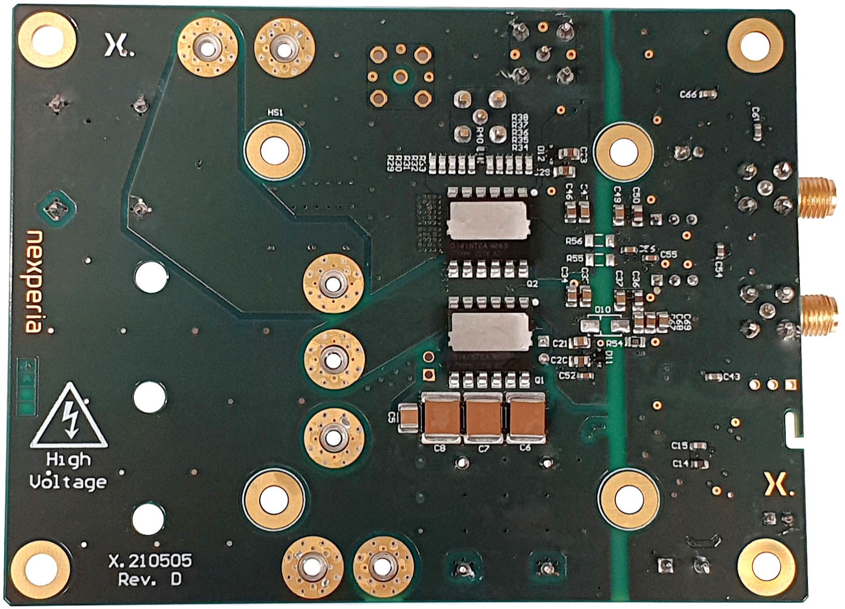
Double pulse evaluation board featuring 33 mΩ GaN FETs in a top-side cooled CCPAK1212i package
The NX-DP-GAN039-TSC double pulse evaluation board enables double-pulse testing of GaN FETs in a top-side cooled copper-clip package (CCPAK). It is optimized for low inductance and features a high-bandwidth current shunt that can be used to evaluate the switching performance with maximum precision. In addition, it can be used for thermal investigations and continuous operation of 5kW and beyond.
Key features & benefits
The Gallium Nitride FET GAN039-650NTB (33 mΩ RDS(on) typ.) used in this evaluation board is a normally-off device, comprised of a high-voltage depletion-mode GaN HEMT (High Electron Mobility Transistor) combined with a tailored 30 V Si-FET in a cascode configuration.It is assembled as a die-on-die stack for best performance and minimized internal parasitics, housed in a 12 mm x 12 mm top-side cooled copper-clip package CCPAK.
Key features of GAN039-650NTB include:
- Very low switching losses
- Rugged gate with high threshold voltage, Vth = 4 V, enables single supply gate drive voltage 0 V to 10 - 12 V.
- Very good QGD/QGS << 1 ratio, protects against parasitic turn-on
- Minimal reverse-recovery
- Very low Rth in top-side cooling for SMD
- Best in class third-quadrant off-state conduction performance for wide-bandgap devices
- Very low package inductance (≈1.3 nH @ 100 MHz)
Key applications
- Solar Inverters
- Energy Storage Systems
- Servo Drives
- Server/Telecom PSU
- Welding Inverters
Products on the board (3)
| Type number | Description | Status | Quick access | |
|---|---|---|---|---|
|
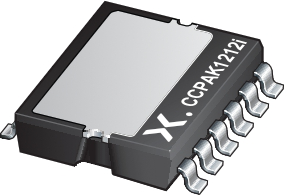
GAN039-650NTB | 650 V, 33 mOhm Gallium Nitride (GaN) FET in a CCPAK1212i package | Production | |

|
74LVC2G14GV | Dual inverting Schmitt trigger with 5 V tolerant input | Production | |
|
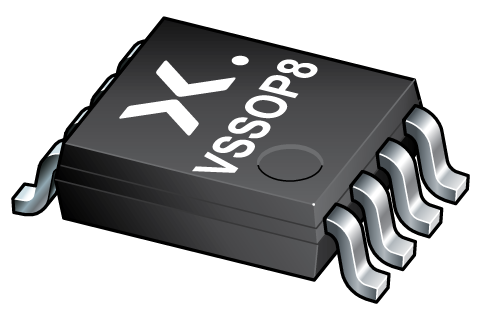
74LVC2G08DC | Dual 2-input AND gate | Production |
Related boards (4)
| Board | Description | Type | Quick links | Shop link | |
|---|---|---|---|---|---|

|
NX-HB-GAN039-TSCUL-top-side-cooled-half-bridge-evaluation-board | 3.5 kW half-bridge evaluation board featuring 33 mΩ GaN FETs in a top-side cooled CCPAK1212i package | Evaluation board | Order | |
|
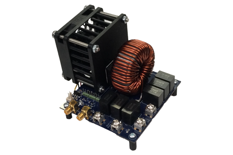
NX-HB-GAN041UL-GAN041-650WSB-half-bridge-evaluation-board | Half-Bridge evaluation board featuring 35 mΩ GaN FETs in a TO-247 package (3.5 kW) | Evaluation board | Order | |

|
NX-HB-GAN039-BSCUL-bottom-side-cooled-half-bridge-evaluation-board | 3.5 kW half-bridge evaluation board featuring 33 mΩ GaN FETs in a bottom-side cooled CCPAK1212 package | Evaluation board | Order | |

|
4-kW-analogue-bridgeless-totem-pole-PFC-evaluation-board | 4 kW analogue bridgeless totem-pole PFC evaluation board | Evaluation board |
Products on the board (3)
| Type number | Description | Status | Quick access | |
|---|---|---|---|---|

|
GAN039-650NTB | 650 V, 33 mOhm Gallium Nitride (GaN) FET in a CCPAK1212i package | Production | |

|
74LVC2G14GV | Dual inverting Schmitt trigger with 5 V tolerant input | Production | |

|
74LVC2G08DC | Dual 2-input AND gate | Production |
Related boards (4)
| Board | Description | Type | Quick links | Shop link | |
|---|---|---|---|---|---|

|
NX-HB-GAN039-TSCUL-top-side-cooled-half-bridge-evaluation-board | 3.5 kW half-bridge evaluation board featuring 33 mΩ GaN FETs in a top-side cooled CCPAK1212i package | Evaluation board | Order | |

|
NX-HB-GAN041UL-GAN041-650WSB-half-bridge-evaluation-board | Half-Bridge evaluation board featuring 35 mΩ GaN FETs in a TO-247 package (3.5 kW) | Evaluation board | Order | |

|
NX-HB-GAN039-BSCUL-bottom-side-cooled-half-bridge-evaluation-board | 3.5 kW half-bridge evaluation board featuring 33 mΩ GaN FETs in a bottom-side cooled CCPAK1212 package | Evaluation board | Order | |

|
4-kW-analogue-bridgeless-totem-pole-PFC-evaluation-board | 4 kW analogue bridgeless totem-pole PFC evaluation board | Evaluation board |
Documentation (2)
| File name | Title | Type | Date |
|---|---|---|---|
| GaNFET_evaluation_board_Terms_Of_Use | GaN FET EVALUATION BOARD TERMS OF USE | Other type | 2023-10-10 |
| UM90028 | NX-DP-GAN039-TSC double pulse evaluation board with top-side cooled CCPAK GaN FETs | User manual | 2024-01-09 |
