Register once, drag and drop ECAD models into your CAD tool and speed up your design.
Click here for more information74CBTLV3257DS-Q100
Quad 1-of-2 multiplexer/demultiplexer
The 74CBTLV3257-Q100 provides a quad 1-of-2 high-speed multiplexer/demultiplexer with common select (S) and output enable (OE) inputs. The low ON resistance of the switch allows inputs to be connected to outputs without adding propagation delay or generating additional ground bounce noise. When pin OE = LOW, one of the two switches is selected (low-impedance ON-state) with pin S. When pin OE = HIGH, all switches are in the high-impedance OFF-state, independent of pin S. To ensure the high-impedance OFF-state during power-up or power-down, OE should be tied to the VCC through a pull-up resistor. The current-sinking capability of the driver determines the minimum value of the resistor.
Schmitt trigger action at control input, makes the circuit tolerant to slower input rise and fall times across the entire VCC range from 2.3 V to 3.6 V.
This device is fully specified for partial power-down applications using IOFF. The IOFF circuitry disables the output, preventing the damaging backflow current through the device when it is powered down.
This product has been qualified to the Automotive Electronics Council (AEC) standard Q100 (Grade 1) and is suitable for use in automotive applications.
Features and benefits
Automotive product qualification in accordance with AEC-Q100 (Grade 1)
Specified from -40 °C to +85 °C and from -40 °C to +125 °C
Supply voltage range from 2.3 V to 3.6 V
High noise immunity
Complies with JEDEC standard:
JESD8-5 (2.3 V to 2.7 V)
JESD8-B/JESD36 (2.7 V to 3.6 V)
5 Ω switch connection between two ports
Rail to rail switching on data I/O ports
CMOS low power consumption
Latch-up performance exceeds 250 mA per JESD78B Class I level A
IOFF circuitry provides partial Power-down mode operation
ESD protection:
HBM: ANSI/ESDA/JEDEC JS-001 class 2 exceeds 2000 V
CDM: ANSI/ESDA/JEDEC JS-002 class C3 exceeds 1000 V
Multiple package options
DHVQFN package with Side-Wettable Flanks enabling Automatic Optical Inspection (AOI) of solder joints
Parametrics
| Type number | Package name |
|---|---|
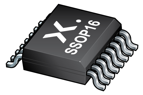
| 74CBTLV3257DS-Q100 | SSOP16 |
Package
All type numbers in the table below are discontinued.
| Type number | Orderable part number, (Ordering code (12NC)) | Status | Marking | Package | Package information | Reflow-/Wave soldering | Packing |
|---|---|---|---|---|---|---|---|
| 74CBTLV3257DS-Q100 | 74CBTLV3257DS-Q10J (935302228118) |
Obsolete | TLV3257 |

SSOP16 (SOT519-1) |
SOT519-1 |
SSOP-TSSOP-VSO-REFLOW
SSOP-TSSOP-VSO-WAVE |
SOT519-1_118 |
Environmental information
All type numbers in the table below are discontinued.
| Type number | Orderable part number | Chemical content | RoHS | RHF-indicator |
|---|---|---|---|---|
| 74CBTLV3257DS-Q100 | 74CBTLV3257DS-Q10J | 74CBTLV3257DS-Q100 |
|
|
Documentation (6)
| File name | Title | Type | Date |
|---|---|---|---|
| SOT519-1 | 3D model for products with SOT519-1 package | Design support | 2023-02-07 |
| cbtlv3257 | IBIS model of 74CBTLV3257 | IBIS model | 2017-12-11 |
| Nexperia_package_poster | Nexperia package poster | Leaflet | 2020-05-15 |
| SOT519-1 | plastic, shrink small outline package; 16 leads; 0.635 mm pitch; 4.9 mm x 3.9 mm x 1.73 mm body | Package information | 2022-06-20 |
| SSOP-TSSOP-VSO-REFLOW | Footprint for reflow soldering | Reflow soldering | 2009-10-08 |
| SSOP-TSSOP-VSO-WAVE | Footprint for wave soldering | Wave soldering | 2009-10-08 |
Support
If you are in need of design/technical support, let us know and fill in the answer form we'll get back to you shortly.
How does it work?
The interactive datasheets are based on the Nexperia MOSFET precision electrothermal models. With our interactive datasheets you can simply specify your own conditions interactively. Start by changing the values of the conditions. You can do this by using the sliders in the condition fields. By dragging the sliders you will see how the MOSFET will perform at the new conditions set.